

A customer came to PCBONLINE for an industrial IoT gateway project with a tight launch date and three supply items to arrive together. The industrial IoT gateway project needed a 12-layer high-speed HDI PCB, an ATS power enclosure, and custom wiring harnesses.
We fabricated the HDI PCB at our own manufacturing bases, sourced the components, assembled and tested the gateway PCBA, and provided the enclosure and harnesses with box-build assembly for the finished IoT gateway. Our engineers reviewed the DFM, managed the sourcing, and kept the production schedule, and the customer worked with one supplier from Gerber review to shipment.
What Is an Industrial IoT Gateway PCBA
An industrial IoT gateway connects field equipment to upper-level networks and the cloud. The PCBA mounts the processor, memory, and ports that move data between the field equipment and the cloud.
The gateway hardware. The assembled gateway PCBA in the photo mounts a processor under an aluminum heatsink, four RJ45 Ethernet ports, and mini-PCIe slots for 4G, 5G, or Wi-Fi modules, with a SIM holder and an SD card slot beside them. Green terminal blocks break out RS-485 and CAN channels for PLCs, meters, and sensors. USB ports, display outputs, and an RTC battery complete the I/O.

Edge computing at the site. The gateway runs Linux on site, next to the machines it monitors. It collects telemetry from serial and Ethernet devices, filters and buffers the data, and pushes it to the cloud over cellular or wired links. When the WAN link drops, the gateway keeps the local control loops alive and uploads the buffered data once the connection returns.
Deployment sites. Substations, production lines, water treatment stations, and energy storage sites all deploy these gateways between fieldbus equipment and the network. The finned aluminum case passively dissipates heat from the processor, so the gateway mounts inside electrical cabinets and on walls without fans or noise.
HDI PCB for Industrial IoT Gateway
The 12-layer high-speed PCB under the industrial IoT gateway is an HDI design, and our own PCB fabrication base in Jiangsu Provinces fabricate it. Laser microvias route the dense processor connections, and back drilling removes the stubs on the high-speed signal paths.
High density. The IoT ga.teway case leaves little room for the PCB, so the PCB designer places microvias under the processor and keeps the power and ground planes unbroken under every BGA. A 0.1 mm laser via fits inside a 0.25 mm pad, and the small pads leave routing channels for the high-speed pairs.
HDI stack-ups and laser vias. Our HDI lines fabricate 1+n+1 to 4+n+4 stack-ups and any-layer HDI up to 16 layers. The table lists the capabilities we apply to industrial IoT gateway PCBs.
|
Item
|
PCBONLINE Capability
|
|
HDI stack-ups
|
1+n+1, 2+n+2, 3+n+3, 4+n+4
|
|
Any-layer HDI
|
Up to 16 layers
|
|
Laser via diameter
|
0.1 mm to 0.25 mm (standard 0.1 mm)
|
|
Laser via aspect ratio
|
1:1 (depth includes copper thickness)
|
|
Laser via fill
|
Plated copper filling (0.1mm-0.125mm vias) or resin filling
|
|
Stacked and staggered vias
|
Up to 5 steps each
|
|
Dimple after copper filling
|
15μm maximum
|
|
Laser via capture pad
|
0.25mm
|
|
Minimum dielectric thickness
|
0.06mm
|
Back Drilling on the 12-Layer High-Speed PCB
A 12-layer high-speed PCB routes Gigabit Ethernet, PCIe, and DDR signals between layers. A plated through-hole via passes through the whole stack-up, and the portion below the connected layer remains as a copper stub. At hundreds of megabits and above, the stub rings at its resonant frequency and reflects energy into the signal path, and the eye diagram at the receiver closes.
Back drilling removes the stub. The drill re-enters the via barrel from the far side and stops at a controlled depth just below the connected layer, so the reflection moves out of the signal band and the eye diagram opens. We back-drill the vias on our own HDI lines, and the DFM review checks the stub length on every high-speed net before fabrication starts.
BOM Sourcing for Industrial IoT Gateway
The gateway BOM covers the processor, memory, Ethernet PHYs, power ICs, connectors, and passive parts. Turnkey PCB assembly at PCBONLINE includes the sourcing, so the customer sends the BOM and receives a costed, sourced version to approve.
Sourcing against the BOM. Our sourcing team quotes each line item through franchise distributors and verified channels, and the Hong Kong procurement team buys each reel at its lowest regional price. Original parts come with date codes and certificates, and the records stay with each production lot.
Alternates for short supply. When a part sits on allocation, we propose alternates with the same footprint and specification. Our engineers review the swap against the circuit, the customer approves the change, and production starts with the confirmed list.
Component risks caught early. A fake or aged component can pass SMT and fail in the field within months. We screen suppliers before the first order, and the incoming inspection checks date codes, markings, and lot certificates before any reel reaches the SMT line.
SMT Assembly for Industrial IoT Gateway PCBA
The 12-layer PCBs finish fabrication at our bases in Jiangsu and Jiangxi Provinces and ship to our turnkey PCB assembly factory in Shenzhen. Our SMT PCB assembly steps are: solder paste printing → solder paste inspection → SMD placement → automatic optical inspection → reflow soldering → automatic optical inspection.
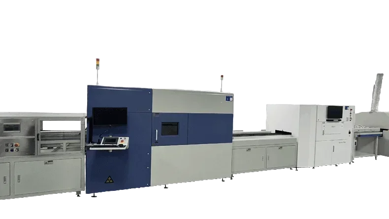
Our SMT assembly for industrial IoT gateways feature:
3D SPI before placement. Solder paste inspection comes first. Our SMT lines inspect every PCB with 3D SPI before placement, and the measurement catches paste volume and alignment offsets before the parts go down.
Placement and reflow. The placement machines set 0201 passives and fine-pitch BGAs, and the reflow profile matches the 12-layer stack, which warms slower than a thin consumer PCB. Our engineers set the profile against the stack-up before the first production run.
Heatsink mounting. The finned heatsink goes onto the processor on the SMT line. Thermal material and clip load follow the work instruction, and a loose heatsink throttles the processor in the field.
3D AOI and X-ray. After reflow, 3D AOI checks every solder joint on every PCB we assemble. The processor and memory BGAs hide their joints under the packages, so 3D X-ray inspects the BGA balls for voids and bridges.
First-article inspection. We inspect a first article before volume production. The FAI confirms the placement program, the feeder setup, and the solder joints on the first assembled PCB, and volume production starts only after the FAI passes.

Box-Build Assembly for Industrial IoT Gateway
The gateway ships as a product, and box-build assembly mounts the PCBA into the enclosure and connects the harnesses. We fabricate the sheet-metal enclosure, build the wiring harnesses, and assemble the finished units in the same program as the PCB.
Sheet-metal enclosures. The gateway PCBAs in the photo sit inside their sheet-metal chassis, screwed down at the standoff points. The RJ45 ports, the display output, and the terminal blocks align with the case cutouts, and the standoff heights follow the mechanical drawing.

ATS power enclosure and harnesses. In the customer project, PCBONLINE also built the ATS power enclosure, the cabinet that switches between two power sources automatically, and the custom wiring harnesses that connect it. The harnesses followed our drawings, and our harness line checked crimp and pull force before installation.
Complete units. The finished gateways in the photo sit on the test benches with finned aluminum lids and power and network cables in place.

Industrial IoT Gateway PCBA Testing
We test at three points, and each point catches a different class of faults. The assembled PCBAs go through functional testing on our benches, then burn-in, then final inspection before packing.
Functional testing. The gateway PCBAs in the photo sit on the benches for functional testing. Each PCBA powers up, and the fixtures check the Ethernet links, the serial channels, the USB ports, and the cellular module. A failed unit goes to the repair station with its test log attached.

IC programming. We program the flash ICs with firmware and OS images on the line, either through our own IC programming service or from an image file the customer supplies. The programming record stays with the production lot.
Burn-in and final inspection. The finished gateways burn in under power in temperature ovens. The burn-in window follows the project requirements, and after burn-in each unit passes a final inspection before packing.
Turnkey Industrial IoT Gateway PCBA: One Engineering Team
Turnkey here means one supplier and one engineering team from Gerber review to shipment, and the customer project shows the difference in three places.
DFM and DFT before fabrication. Our engineers review the stack-up, the back-drill depths, and the test points before fabrication starts. The DFM and DFT reviews catch risks early in development, when a change costs a revision instead of a redesign.
IPC Class 3 process controls. We assemble the gateway PCBAs under IPC Class 3 process controls, the acceptance class for high-reliability industrial and server electronics. The same controls set the solder joint acceptance, cleanliness, and inspection criteria on the SMT line.
Fewer handoffs, predictable delivery. Our engineering team coordinated the HDI fabrication, the sourcing, the enclosure, the harnesses, and the assembly for the customer project. The customer worked with one supplier, the schedule moved without supplier-to-supplier waiting, and the launch date held.
Choose PCBONLINE for Your Industrial IoT Gateway PCBA
PCBONLINE provides one-stop industrial IoT gateway PCBA manufacturing, including HDI PCB fabrication, component sourcing, PCB assembly, box-build assembly, and testing.

Founded in 2005, PCBONLINE has two large PCB manufacturing bases in Jiangsu and Jiangxi Provinces and a turnkey PCB assembly factory in Shenzhen.
HDI PCB fabrication from 1+n+1 to 4+n+4 and any-layer up to 16 layers, with back drilling for high-speed signals.
Component sourcing with alternative part proposals through our Hong Kong procurement team.
SMT assembly with 3D SPI, 3D AOI, and 3D X-ray inspection, and a first-article inspection before volume production.
Box-build assembly with custom sheet-metal enclosures and wiring harnesses.
IC programming, functional testing, and burn-in testing before shipment.
PCBA manufacturing certified with ISO 9001:2015, ISO 14001:2015, IATF 16949:2016, RoHS, REACH, UL, and IPC-A-610 Class 2/3.
Send your Gerber files and BOM to info@pcbonline.com, and our engineering team replies with a DFM report and a quotation for your industrial IoT gateway project.
FAQs About industrial IoT gateways
Q: What does turnkey PCB assembly include for an industrial IoT gateway?Turnkey PCB assembly covers HDI PCB fabrication, component sourcing, SMT assembly, box-build assembly with the enclosure and harnesses, IC programming, and testing. PCBONLINE delivers all of these under one engineering team.
Q: Why does an industrial IoT gateway need an HDI PCB?The gateway packs a processor, memory, and many ports into a small fanless case. HDI microvias and fine lines provide the density, and they keep the power and ground planes unbroken under the processor.
Q: Why is back drilling needed on a 12-layer high-speed gateway PCB?A through-hole via leaves a copper stub below the connected layer, and the stub reflects energy at high signal speeds. Back drilling removes the stub to a controlled depth and keeps the eye diagram open.
Q: Can PCBONLINE build the enclosure and wiring harnesses together with the gateway PCBA?Yes. PCBONLINE builds sheet-metal enclosures, ATS power enclosures, and custom wiring harnesses in the same program as the PCB fabrication and assembly.
Q: Which quality standards apply to industrial IoT gateway PCBAs at PCBONLINE?Industrial IoT gateway PCBAs ship to IPC-A-610 Class 3 acceptance, and the factories hold ISO 9001:2015, ISO 14001:2015, IATF 16949:2016, RoHS, REACH, and UL certifications.
PCB assembly at PCBONLINE.pdf


