

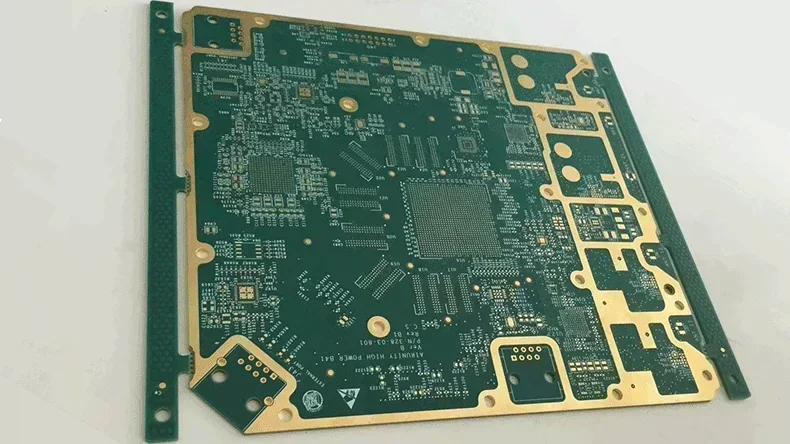
China fabricates 70% to 80% of the world's AI server GPU PCBs. The manufacturers cluster in South China, close to the SMT assembly lines. An AI server motherboard starts as a 24+ layer HDI PCB and ends as a tested PCBA that seats eight GPUs.
An AI server motherboard is a young product category. Electronic engineers and sourcing managers ask us almost the same questions in the first email: How many layers, which laminate, which surface finish, and whether we fabricate and assemble the AI server PCBs in one place.
An AI server motherboard leans hard on the junction between PCB fabrication and assembly. The PCB process sets the ENIG pad surface, the PCB flatness through reflow, and the bevel on the edge connectors. After PCB fabrication, the bare PCBs ship to our turnkey PCB assembly factory for SMT.
What Is an AI Server Motherboard?
An AI server motherboard is the large carrier PCB inside an AI training or inference server. It seats the CPU sockets, the GPU modules, the DRAM, the NVMe storage, and the network interfaces. It also distributes hundreds of amps to each processor through dense voltage regulator zones.
A training AI server motherboard runs two CPU sockets and eight GPU modules. Each GPU draws 400 W to 700 W, and the PCB under them routes tens of thousands of nets between GPUs, CPUs, and memory at 32 GT/s and higher. All the routing fits on a PCB about 3 mm thick.
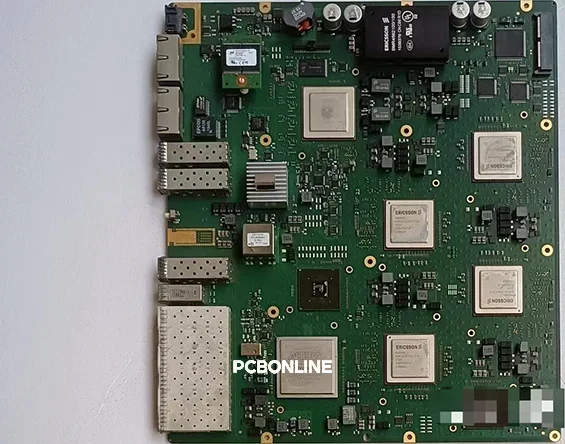
The GPU seats. Each GPU lands on a land pattern with thousands of pads. Coplanarity across that pattern comes from the surface finish, so the finishing process at the fab determines whether the solder joints form cleanly at reflow.
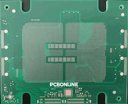
The power tree. A 54 V DC input from the power shelf feeds multi-phase voltage regulators. Each regulator converts the 54 V bus down to a 0.8 V core rail and delivers hundreds of amps per GPU. The PCB layers under each regulator zone carry that current, so copper weight and pour geometry become stack-up decisions, not afterthoughts.
The thermal path. GPU heat enters the PCB through the package balls and the thermal via field under each die. Copper planes spread that heat through the stack, and the PCB works as part of the cooling system alongside the heatsink and the cold plate.
Why AI Server PCBs Run 24+ Layers
The net count determines the layer count. A dual-socket server motherboard routes thousands of differential pairs between GPUs, CPUs, and memory. Each pair routes against a solid reference plane. With 24+ PCB layers, an AI server PCB has enough space to add the power planes and the ground planes that the pairs reference.
HDI inner-layer interconnect. Mechanical through-holes waste routing channels on a dense PCB. Laser-drilled microvias connect layers directly and stack through the HDI regions, which shortens the escape routing under each BGA. GPU PCBs sit at the top of the industry. Their stack-ups, microvia structures, and registration tolerances all push standard process limits.
Fine lines and tight spaces. An AI server PCB etches 3 mil lines and spaces on outer layers and packs 0.8 mm pitch BGAs with via-in-pad structures. The traces between a GPU and its memory run inside regions a few millimeters wide, and every mil of spacing comes back as routing channel. Precision etch is the reason these PCBs stay hard to copy.

Production panel of AI server accelerator cards with large gold planes and dense BGA pad fields
Back-drilling. A through-via that spans 24 layers leaves a stub when it only connects the top layers. The stub reflects high-speed signals and degrades eye diagrams at 32 GT/s. Back-drilling removes the stub from the underside, and the fab controls the depth to within a few mils of the target layer.
Low-loss laminate. Standard FR-4 absorbs too much signal at multi-GT/s rates. AI server PCBs use Megtron 6 class laminates with low dissipation factor, and the press cycle for those materials runs tighter temperature and pressure windows than a standard FR-4 cycle.
Stack-Up: Materials, Copper Weights, and Warp Control
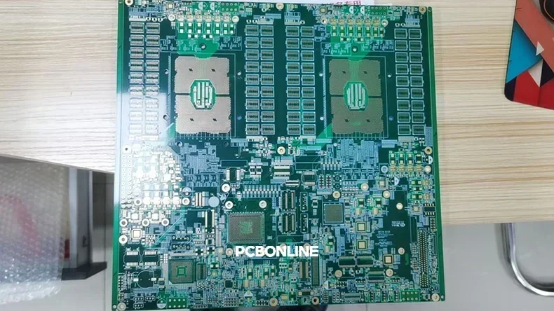
Bare 24-layer AI server PCB with two LGA CPU sockets before SMT assembly
In an AI server motherboard project, the stack-up drawing is one of the most important documents. It sets the layer order, the copper weights, the dielectric thicknesses, and the impedance targets.
Balanced construction. A symmetric stack-up keeps the PCB flat through lamination. An asymmetric one bows, and the warp shows up later at reflow and pulls on BGA balls until they crack. The AI server motherboard in the photo carries two CPU sockets and a full HDI field, and it stays flat because the copper and dielectric layers balance around the core.
Power layers, precision etched. An AI server motherboard carries rail current in wide copper pours etched on standard power layers, mostly 1 oz to 2 oz copper. Heavy copper plating is rare on server PCBs, because the routing density leaves little room for it. The pours run wide and flat, the VRM layout splits current across parallel phases, and the pour shapes spread current density before it concentrates at any via.
Press and registration. A 24-layer HDI PCB stacks microvias across multiple layers, and each stacking step adds a tolerance.We track layer-to-layer registration on every production panel, because a stacked microvia that lands off-target becomes a latent open that no electrical test at the bare-PCB stage can catch.

A production panel carrying five AI server PCBs with ENIG gold-frame openings and edge connectors
Heat Dissipation: The PCB Side of GPU Cooling
An 8-GPU AI server motherboard pushes several kilowatts of heat into its cooling system.

The above whiteboard in our engineering review lists the air side of that budget next to the power side, 6 CPUs and 96 fans for the 24 kW build. The cold plates and heatsinks take the headline role. The PCB carries heat through drilled thermal vias and unbroken copper planes, and the laminate holds its dimensions at high temperature.
Thermal via fields. Each GPU seat carries an array of thermal vias under the die. The vias tie the package pads to the internal copper planes and move heat down into the stack. Drill diameter, via plating, and array density all get fixed in the stack-up review, alongside the signal escape routing that shares the same area.
Plane layers as heat spreaders. Continuous copper planes spread heat laterally across the PCB. Ground and power planes stay unbroken under each GPU seat, and the CAD review keeps slot cuts and plane splits out of the GPU fields. A plane that stays whole spreads heat; a plane chopped into islands turns into a hot spot.
Low-CTE, high-Tg materials. A GPU junction swings from room temperature past 90 °C under load, and every cycle expands the package and the PCB at different rates. CTE mismatch stresses the BGA balls, and low-CTE, high-Tg laminates keep the PCB dimensionally stable across years of those cycles. The same mechanism shortens joint life in service. A stack-up that drifts with heat eventually cracks a ball.
Mounting and flatness. Cold plates and heatsinks clamp the PCB with real force. Standoff loads, torque specs, and the flatness of the mating surfaces all get engineered against warp, because a PCB that bows under clamp load brings the reflow warp problem back in service.

Surface Finish: ENIG and Edge Connectors
Surface finish is the last PCB manufacturing step. On an AI server motherboard, the finish has to keep thousands of BGA pads flat and solderable, and it has to keep the edge connectors working through years of mating cycles.
ENIG under every BGA. ENIG plates nickel 3 to 6 µm thick and tops it with 0.05 to 0.1 µm of immersion gold. The finish gives a flat pad surface for the large BGA packages, and a GPU seat demands that flatness. Nickel thickness and bath chemistry determine how the joint survives thermal cycling. A thin or contaminated nickel layer builds a brittle intermetallic, and the first few hundred thermal cycles crack the solder ball. The PCBA runs fine at final test and fails months later in the field. That sequence starts at the plating tank.
Edge connector wear. Gold fingers on a server PCB mate and unmate through maintenance cycles for years. Hard gold over a nickel barrier layer resists that wear; thin gold wears through, contact resistance climbs, and the link drops. Edge connectors also need a bevel on the leading edge, and the bevel cut happens after electroplating at our hard gold line.

AI server accelerator cards with ENIG gold planes and gold finger edge connectors
The finishing line. We run the ENIG line and the hard gold edge-plating line in our Jiangxi PCB manufacturing base. ENIG deposits nickel and gold by chemical immersion, and hard gold plates by electroplating. We don't outsource any manufacturing step.
SMT Assembly for AI Server Motherboard
A 3 mm, 24-layer HDI motherboard behaves differently on an SMT line than a 1.6 mm consumer PCB. It warms slower in the oven, warps under thermal gradient, and demands tighter coplanarity at the GPU seats. Our SMT lines run 3D SPI and 3D AOI on every PCB we assemble, and every order starts with a first-article inspection before volume production.
Solder paste inspection. SPI measures the volume, height, and position of every paste deposit before placement. Paste volume varies with warp and with stencil separation quality across a PCB this size, so SPI data catches process drift before it reaches the oven.
Reflow on a heavy PCB. The 3 mm stack warms slowly and cools slowly. The reflow profile has to drive enough heat into the core and still hold the surface packages below their limit. Gradients across the PCB warp it, and warping during the liquidus phase pulls on BGA balls. The bare PCB was flat at electrical test. The oven is the step that bends it.
3D X-ray on every BGA. Solder voiding hides under the package body. 3D X-ray measures each void against the pad area, and IPC-7095 sets the acceptance limit at 25%. A line that only samples skips the one defect class most likely to shorten GPU joint life.
First-article inspection. Before volume, the line assembles one unit and cross-sections it at the GPU seats, the CPU sockets, and the thermal via fields. When a first article fails, the stack-up engineer from the PCB plant joins the SMT engineers, and the two teams read the same cross-section together. That meeting closes the loop between fabrication data and assembly data.

Production panel with eight numbered AI server accelerator cards
Power Delivery: Precision Pours and the 24 kW Harness
Inside the AI server motherboard, power moves through etched copper. Outside it, power becomes a mechanical engineering problem. For a 24 kW AI server node, 32 A × 380 V works out to 12 kW per branch, 63 A × 380 V to 24 kW, and 105 A × 380 V to 48 kW for a full cabinet. Each step up in service current doubles the copper cross-section in the cable, and each step moves the connector class up with it.
Custom harnesses and connectors. Above 24 kW, the harness is a design object, not an accessory. PCBONLINE engineers the harness and connector set for a 24 kW AI server and a partner factory produces it to our drawings. The set includes CEE-form inlet connectors on 5-core high-flex cable, rated for continuous node current with margin. The derating calculations, the crimp specifications, and the acceptance tests sit with our engineering team, on the whiteboard page next to the branch math.

Connector and cable selection. Every conductor runs below its ampacity rating at the cabinet ambient temperature. Contact plating, insertion force, and retention force all get specified per mating cycle count, because a node gets serviced and re-cabled across its service life.

AI Server Motherboard Testing
An AI server motherboard passes comprehensive tests during PCB fabrication and assembly. Fabrication testing checks the PCB, assembly inspection checks the solder joints, and functional test and burn-in check the finished PCBA.
Bare-PCB electrical test. We test every net on every production panel for continuity and isolation, against the netlist from the Gerber data. An impedance coupon goes through the press with each production panel, and we report the coupon values with each production lot.
Assembly inspection. 3D AOI checks every component after placement and again after reflow. Solder joint geometry, component offset, and coplanarity all get measured in three dimensions.
Functional test and firmware. After assembly, the line flashes firmware and runs a functional test on each PCBA. A functional test on a motherboard covers the management controller, the power sequencing, and the link training on the high-speed lanes.
Burn-in. Powered aging at elevated temperature screens infant mortality failures. Units that survive burn-in go to final test, and the production record stays attached to each serial number.
Choose PCBONLINE to Build Your AI Server Motherboards
PCBONLINE provides one-stop AI server motherboard manufacturing, including HDI PCB fabrication and assembly, box-build assembly, custom connectors, and custom cables.

Founded in 2005, PCBONLINE has two large advanced PCB manufacturing bases and one PCB assembly factory, with its headquarters in Shenzhen.

AI server PCB fabrication with HDI via-in-pad copper filling for GPU designs with 24+ layers.
We provide one-stop AI server PCB manufacturing, including component sourcing, PCB fabrication, assembly, testing, and system integration.
SMT assembly with fine-pitch BGA placement accuracy and custom reflow profiles for warpage-free soldering.
100% X-Ray inspection, functional testing, and burn-in testing for guaranteed reliability.
We have rich experience in impedance control, oven temperature control, and assembly fixture designs.
Supporting IC programming in the cloud, controlled by you, and protecting your intellectual property.
High-quality OEM PCBA manufacturing certified with ISO 9001:2015, ISO 14001:2015, IATF 16949:2016, RoHS, REACH, UL, and IPC-A-610 Class 2/3.
China supplies 70% to 80% of global AI server GPU PCBs, and PCBONLINE stands out as a reliable turnkey AI server motherboard manufacturer. At PCBONLINE, we can help our clients reduce costs while achieving the highest levels of performance and reliability. If you are interested in AI server motherboards from PCBONLINE, send your inquiry by email to info@pcbonline.com.
How to Choose an AI Server Motherboard Manufacturer
Ask questions about the six aspects below before you release an AI server motherboard project to a factory.
Layer count and HDI depth. Ask for 24+ layer references with any-layer HDI and measured impedance reports from recent projects. A PCB manufacturer that runs 24 layers but subcontracts its HDI drilling adds a handoff at the HDI drilling step, where the tolerances are tightest.
Finishing lines in-house. ENIG and hard gold edge plating on the manufacturer's own lines shorten the loop between plating data and fabrication data. Ask which plating lines the manufacturer owns and which get subcontracted.
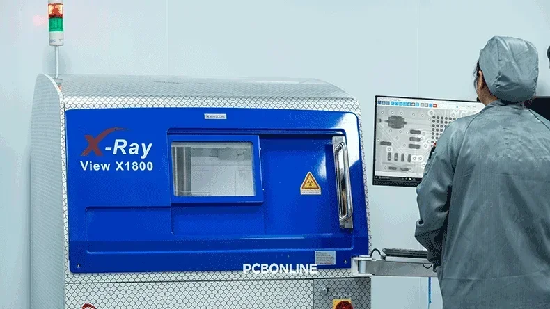
X-ray with void reporting. Request a sample X-ray report from a BGA-heavy production run. The report should show void percentages per joint, per IPC-7095.
Thermal and material range. Ask for low-CTE, high-Tg material options and thermal via field references from GPU-class projects. Ask how the manufacturer reviews heatsink mounting loads against PCB flatness.
Power engineering. A manufacturer that engineers harnesses and connectors alongside the PCB can size the 12 kW, 24 kW, and 48 kW branches with the motherboard, in one project.
First-article discipline. Ask how the factory runs first articles and who attends the inspection. You want the answer to name the stack-up engineer.
Frequently Asked Questions About AI Server Motherboards
Q: How many layers does an AI server PCB have?Mainstream AI server motherboards for training run 24 or more layers, and high-end designs push higher. Layer count rises with net density, GPU count, and the number of reference planes the high-speed pairs require.
Q: Why are most AI server PCBs built in China?China produces 70% to 80% of the world's AI server GPU PCBs. The concentration comes from HDI capacity at 24+ layers, a mature low-loss laminate supply chain, and dense SMT capacity nearby, so fabrication and assembly stay inside one engineering loop.
Q: How do AI server PCBs dissipate GPU heat?Heat enters the PCB through thermal via fields under each GPU and spreads through continuous copper planes. Low-CTE, high-Tg laminates keep the PCB dimensionally stable across thermal cycles, and the stack-up keeps the cold plate mounting surfaces flat under clamp load.
Q: What surface finish works best for an AI server motherboard?ENIG suits the large BGA packages because the pad surface stays flat for coplanarity. Edge connectors need hard gold over a nickel barrier for insertion wear. PCB manufacturers run the two finishes on separate plating lines, ENIG by chemical immersion and hard gold by electroplating.
Q: How much power does one AI server node draw?A single 8-GPU training node draws roughly 10 kW to 12 kW at the wall. A 24 kW branch service (63 A × 380 V, three-phase) supplies a full node with margin, and a 105 A × 380 V feed covers a 48 kW cabinet.
PCB assembly at PCBONLINE.pdf


