
Designing a PCB (printed circuit board) is more than just connecting components with traces; it requires a strategic balance between physical constraints and electrical performance. Two critical aspects of this design process are the form factor and the requirements for component placement. The form factor and component placement dictate the board's physical appearance, influence functionality, thermal performance, manufacturability, and cost.
This article delves deep into the significance of PCB form factor and component location requirements, offering insights into best practices, industry standards, and real-world design considerations that every engineer, developer, and designer should know.
In this article:
Part 1. What Is a PCB Form Factor? Part 2. PCB Component Placement: More Than Just Positioning One-stop OEM PCB Manufacturer With One-on-One Engineering SupportWhat Is a PCB Form Factor?
The form factor of a PCB refers to the physical dimensions, shape, and mounting layout of the board.
It defines the envelope within which the entire circuit must be housed and determines how the PCB fits within the larger product or system.
Whether a board is rectangular, circular, or highly irregular, the form factor sets the stage for every other design consideration.
Common types of form factors
- Standard rectangular PCBs: Widely used due to ease of manufacturing and compatibility with standard enclosures. A rectangular PCB for industrial controls should meet strict thermal and EMC requirements while fitting inside a compact DIN rail housing.
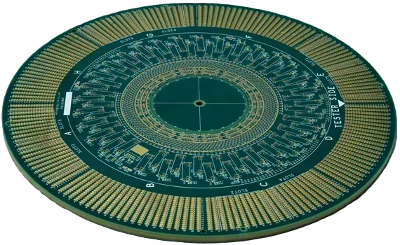
- Circular PCBs: Found in products like watches, sensors, and small embedded devices. A circular PCB in a smartwatch required tight component placement, efficient power management, and alignment with the display and sensors.
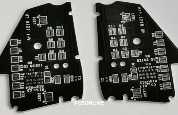
- Irregular shapes: Custom-shaped PCBs that fit specific product housings or optimize space utilization. A small, irregular-shaped PCB for an IoT sensor node should balance battery, RF, and MCU placement for optimal wireless performance.
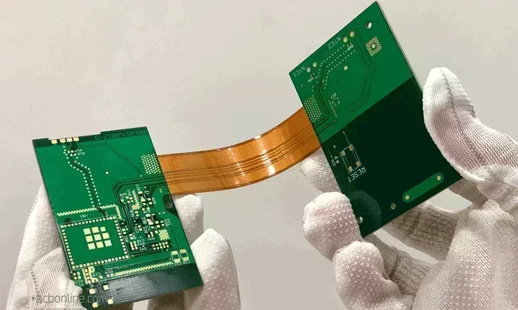
- Rigid-flex PCBs: Combine rigid and flexible sections, allowing three-dimensional packaging and reducing connector needs.
Why form factor matters
The form factor impacts:
- Enclosure compatibility
- Thermal management
- Aesthetic design
- Electrical signal integrity
- Manufacturing constraints and cost
Choosing the right form factor from the beginning can prevent costly redesigns later in development.
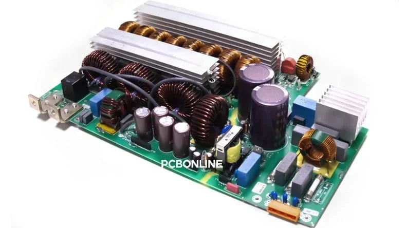
PCB Component Placement: More Than Just Positioning
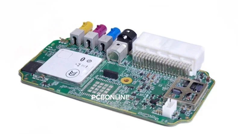
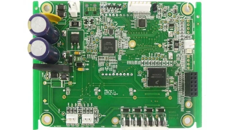
Component placement is a cornerstone of effective PCB design. It refers to the strategic arrangement of electronic components on the board surface to ensure functionality, reliability, and manufacturability.
Key placement considerations are below.
Signal integrity
Signal integrity and EMC are closely tied to how components are placed and routed. High-speed signals require short and direct routing to minimize noise and crosstalk.
Best practices:
- Avoid sharp corners in traces.
- Keep high-speed lines away from analog sections.
- Route differential pairs together with consistent spacing.
- Place ground planes under sensitive circuits.
- Use guard traces and shielding cans where necessary.
Thermal management
Heat is a major enemy of electronic reliability. Poor component placement can lead to localized hotspots and premature component failure.
Heat-generating components should be spaced appropriately and located near heat sinks or vents.
To ensure thermal dissipation, simulate the thermal behavior. Modern EDA (Electronic Design Automation) tools offer simulation, constraint checking, and visualization capabilities that help optimize component layout. EDA tools can simulate thermal behavior, allowing designers to test different placements virtually before finalizing the layout.
Strategies for better heat dissipation:
- Place high-power components near heat sinks.
- Use thermal vias to transfer heat to inner or opposite board layers.
- Ensure sufficient airflow paths in the layout.
Serviceability
Components that may need replacement or adjustment should be easily accessible.
Start placement with fixed-position components (e.g., connectors).
Use silkscreen labels for easier assembly and debugging.
Always check the 3D model against the enclosure.
Electrical priorities
The challenge in PCB design lies in balancing the electrical performance requirements with physical limitations.
For instance, placing a capacitor close to a power pin improves electrical performance but may conflict with space constraints or thermal paths.
High-speed signal lines should be as short and direct as possible.
Sensitive analog components should be isolated from noisy digital circuits.
Decoupling capacitors should be placed close to power pins.
Power supply components should be placed to ensure even and stable power delivery.
Physical layout
Place larger and taller components first.
Group related components by function (e.g., power section, microcontroller, sensors).
Maintain symmetry for balanced current flow and aesthetic alignment.
Connectors, buttons, and displays must align with enclosure cutouts or mechanical supports.
Meeting industry standards and guidelines
Designing a PCB to meet industry standards ensures compatibility, reliability, and regulatory compliance.
IPC standards include
- IPC-2221: Generic standard for PCB design.
- IPC-7351: Guidelines for surface mount land pattern design.
- IPC-6012: Qualification and performance specification for rigid PCBs.
Manufacturer guidelines
Most PCB fabricators and assemblers provide design specifications regarding:
- Minimum trace width and spacing
- Drill hole sizes
- Board thickness
- Component clearance
Avoid these common mistakes
- Ignoring component height limits
- Overcrowding the board
- Neglecting the thermal path
- Misplacing polarized components
One-stop OEM PCB Manufacturer With One-on-One Engineering Support
If you're looking for a professional PCB manufacturer that can provide one-on-one engineering support for your project, you can work with the advanced PCB manufacturer PCBONLINE from R&D to one-stop PCBA manufacturing and box-build assembly from prototypes to massive production.

Founded in 1999, PCBONLINE has two large advanced PCB manufacturing bases, one turnkey PCB assembly factory for PCB assembly and box-build assembly, stable material supply chains and strategic cooperation with electronic component manufacturers, and long-term cooperation with the top 3 mold and enclosure manufacturers in China for jigs/fixtures, molds, and enclosures.
Besides, PCBONLINE has an R&D team and professional CAM engineers for project development and DFM (design for manufacturing).
In the DFM stage, PPCBONLINE will carefully check your Gerber and BOM to ensure the PCB component placement, form factor, etc., meet the manufacturability requirements.
PCBONLINE can provide R&D or take part in the development of your project, including PCB layout, structural engineering, testing, the enclosure, and solving technical issues.
PCBONLINE manufactures, assembles, and tests from PCBs to box builds as a source factory manufacturer under one roof, from prototypes to bulky production.
Turnkey electronic manufacturing capabilities under one roof, including PCB fabrication, component sourcing, PCB assembly, tests, enclosures, box-build assembly, labelling, and shipping.
Complete PCBA value-added services in the post-assembly stage, including conformal coating, functional test, thermal aging, IC programming, box-build assembly, and application simulation testing.
High-quality PCBA manufacturing certified with ISO 9001:2015, ISO 14001:2015, IATF 16949:2016, RoHS, REACH, UL, and IPC-A-610 Class 2/3.
When your project enters the bulky production stage, PCBONLINE refunds the fees of prototyping, including its value-added services.
Whether you are designing for wearables, industrial systems, IoT devices, and so on, you can work with PCBONLINE to optimize your PCB's form factor and component placement and yield satisfying results. To get a quote from the turnkey PCBA manufacturer PCBONLINE, contact info@pcbonline.com.
Conclusion
Form factor and component placement are foundational to successful PCB design. They influence every aspect of a device's performance, reliability, and user experience. By carefully considering shape, space, signals, and standards, designers can create PCBs that not only function flawlessly but also integrate seamlessly into their final products. To ensure the success of your PCB/PCBA projects, work with the turnkey advanced PCB manufacturer PCBONLINE.
PCB fabrication at PCBONLINE.pdf


