
In the realm of Printed Circuit Boards (PCBs), dielectric strength is a critical parameter that influences performance, safety, and longevity.
Dielectric strength refers to the maximum electric field a material can endure without electrical breakdown.
Measured in units such as V/mil or kV/mm, it defines the insulating capacity of the materials used between conductive layers.
A high dielectric strength ensures robust insulation, which is vital for preventing short circuits and preserving signal integrity in electronic applications.
This article delves deep into dielectric strength as it relates specifically to PCBs, moving beyond general concepts to focus on materials, structure, fabrication quality, and practical testing approaches.
PCB Materials and Their Dielectric Strength
What Is Dielectric Strength? Dielectric strength is defined as:
"The maximum voltage that an insulating material can withstand before it experiences electrical breakdown."
In PCBs, dielectric materials are layered between conductive copper traces to isolate and insulate them. If the dielectric strength is exceeded, the insulation fails, causing current to pass through where it shouldn't, leading to failure or permanent damage.
The dielectric strength is usually expressed in:
- Volts per mil (V/mil) in the imperial system
- Kilovolts per millimeter (kV/mm) in the metric system
A typical dielectric material like FR4 has a dielectric strength of about 500 V/mil or 20 kV/mm, while other PCB substrate materials like PTFE (Teflon) or PI (Polyimide) exhibit even higher values.
The substrate material used in PCB fabrication plays the most critical role in determining the board’s overall dielectric strength.
Below is a table of the dielectric strength of common PCB materials.
|
Material
|
Dielectric Strength (approx.)
|
|
PTFE
|
500–700 V/mil (20–28 kV/mm)
|
|
PI (Polyimide)
|
300–500 V/mil (12–20 kV/mm)
|
|
FR4
|
300–500 V/mil (12–20 kV/mm)
|
|
Ceramics
|
100–200 V/mil (4–8 kV/mm)
|
|
Metal-core dielectric
|
<100 V/mil (~4 kV/mm)
|
|
Copper/Aluminum
|
0 (conductive, not dielectric)
|
How to Test Dielectric Strength in PCBs
Standard Dielectric Withstanding Voltage (DWV) tests apply a gradually increasing voltage across the insulating layers, monitor for leakage current, and identify the voltage at which breakdown occurs.
The typical dielectric strength testing method uses a dielectric strength tester.
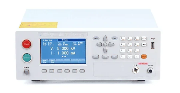
When testing the PCB dielectric strength, connect the probe of the dielectric strength tester to the contact pad of the PCB.
On the dielectric strength tester, custom set up the testing time, a certain high voltage, and the start and end values of the current range.
Then, power on the dielectric strength tester, which will gradually increase the current from the start value to the end value at a certain voltage.
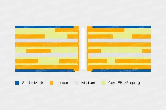
Dielectric Breakdown and Insulation Layer Thickness
Dielectric breakdown occurs when the electric field within a dielectric exceeds its threshold, leading to a sudden surge of current. This is often irreversible and marks the failure point of the material. It’s influenced by several factors:
- Material properties (intrinsic strength, molecular structure)
- Layer thickness (d)
- Voltage stress applied over time
- Manufacturing defects
- Moisture, contamination, and air bubbles
The dielectric strength of a PCB increases with the thickness of its insulation layers. A thicker layer offers a longer path for electricity to traverse before causing breakdown.
However, designers must find a balance:
- Too thin, and the risk of breakdown increases.
- Too thick, and the PCB becomes bulky, raising manufacturing costs and introducing challenges for high-speed signals.
Designing a PCB with adequate dielectric strength requires balancing:
- Number of layers
- Overall board thickness
- Signal integrity
- Mechanical stability
- Cost and fabrication ease
PCB Layer Management and Its Impact
Good layer management involves:
- Consistent layer separation
- Strategic signal and ground plane allocation
- Controlled impedance matching
This ensures that dielectric materials function within safe operating conditions, reducing the chances of breakdown.
Importance of Dielectric Strength in High-Frequency PCBs
Dielectric strength can be significantly impacted by the quality of PCB fabrication. Even the best materials will fail if:
- The lamination process traps air
- There are voids between layers
- Foreign contaminants are present
The methods to ensure PCB quality regarding dielectric strength include:
- Vacuum lamination
- Laser direct structuring
- Automated optical inspection (AOI) after each conductive layer is etched
In high-frequency PCBs, dielectric performance is even more critical. The reasons are that signal loss increases with poor insulation, and high-frequency signals are more sensitive to impurities, holes, and voids.
The critical points in high-frequency PCB manufacturing for enhancing dielectric performance include:
- Plasma cleaning to remove organic residues.
- Avoidance of voids and bubbles.
- Use of homogeneous, high-quality dielectric materials.
To ensure high dielectric strength in PCBs:
- Select the right substrate: PTFE and PI for high-performance, FR4 for general use
- Ensure proper insulation thickness based on voltage requirements
- Prioritize fabrication quality
- Use plasma cleaning and high-frequency PCB techniques where needed
- Balance dielectric performance with practical design constraints
Turnkey PCB Manufacturer with R&D without Dielectric Strength Hassles
How do you ensure the PCB material and layer thicknesses make a good balance between dielectric strength and PCB space requirements? You can work with a reliable turnkey PCB manufacturer, PCBONLINE, with R&D and EMS (electronic manufacturing service) capabilities.

Founded in 1999, PCBONLINE has two large advanced PCB manufacturing bases, one turnkey PCB assembly factory for PCB assembly and box-build assembly, stable material supply chains and strategic cooperation with electronic component manufacturers, and long-term cooperation with the top 3 mold and enclosure manufacturers in China for jigs/fixtures, molds, and enclosures.
Besides, PCBONLINE has an R&D team and professional CAM engineers for project development and DFM (design for manufacturing).
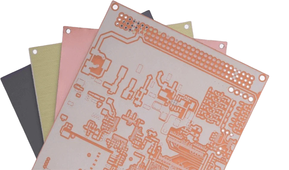
PCBONLINE can manufacture various types of PCBs with materials of dielectric strength proper for the application requirements, including FR4, PTFE, ceramics, PI, aluminum, copper, PET, and even glass.
Provides one-on-one free and professional DFM (design for manufacturing) for PCB, PCBA, and box-build projects, ensuring the PCB dielectric strength and performance.
PCBONLINE manufactures, assembles, and tests from PCBs to box builds as a source factory manufacturer under one roof, from prototypes to massive production.
Rich experience in high-current and high-voltage PCB/PCBA projects with high dielectric strength requirements, such as industrial controls, battery management systems, etc.
High-quality PCBA manufacturing certified with ISO 9001:2015, ISO 14001:2015, IATF 16949:2016, RoHS, REACH, UL, and IPC-A-610 Class 2/3.
When your project goes to the bulky production stage, PCBONLINE refunds the fees of prototyping, including its value-added services.
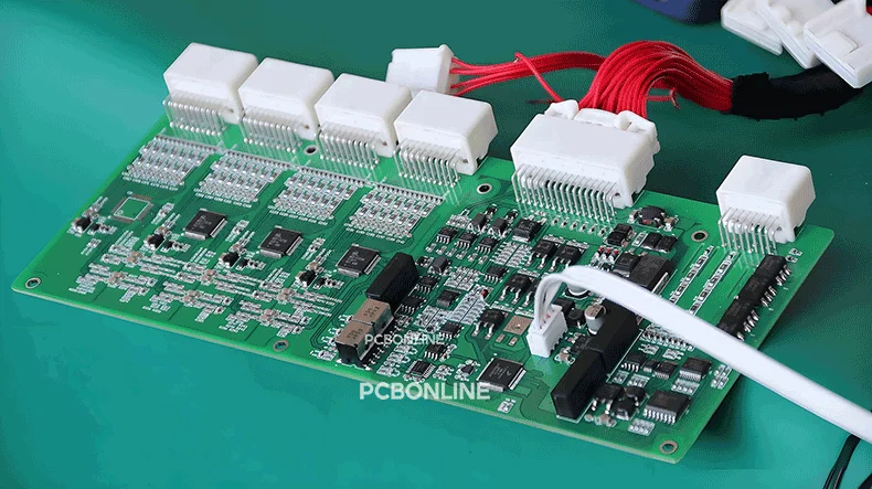
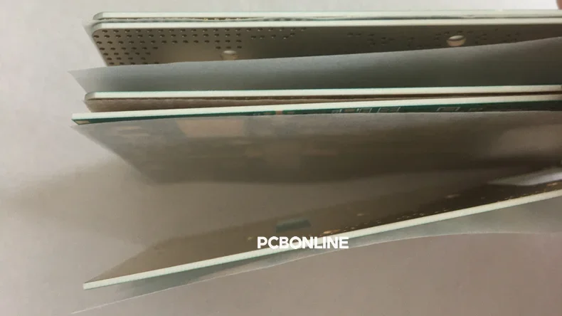
Examples of PCBs with high dielectric strength requirements
Below are two LED PCBs with high dielectric strength manufactured and tested by PCBONLINE.
We tested the two LED PCBs under the 1.5KV voltage from 1.0mA to 100mA currents for 1 minute. Below is the dielectric strength tester we used in testing the electrical breakdown of the two PCBs.
It turned out that both LED PCBs can withstand the 1.5 kV high voltage and have good insulation and dielectric strength.
By working with the one-stop PCBA manufacturer PCBONLINE, you can ensure the balance between dielectric strength, insulation, and thickness with our professional DFM and one-on-one engineering support. No matter what application the PCB will be used for, such as automotive, industrial, medical, military, aerospace, communication, etc, you can work with PCBONLINE. To get a quote for your project from the turnkey PCBA manufacturer PCBONLINE, contact info@pcbonline.com.
Conclusion
Understanding and managing dielectric strength in PCBs ensures safety, reliability, and performance in all electronic applications—from everyday consumer electronics to high-frequency aerospace systems. To ensure the success of your PCB and PCBA project with a good balance between dielectric strength and thickness, work with the one-stop advanced PCB manufacturer PCBONLINE.
PCB fabrication at PCBONLINE.pdf


