
Amplifiers are vital components in electronic circuits used in countless devices that amplify signals (analog signals, digital signals, sounds, voltage, power, light, etc). Whether it's boosting the volume of a sound signal, amplifying weak sensor readings, or driving high-power loads, amplifiers come in various types and configurations tailored to meet specific application requirements.
In this article, we delve into the fundamentals of printed circuit board (PCB) amplifiers, exploring their operation, classification, and design considerations! You can also find an box build assembly manufacturer that can turn your amplifier PCB design into real products.
In this article:
Part 1: What is an Amplifier Part 2: Classes of Amplifiers Part 3: Amplifier PCB Circuit Example – Single Stage Voltage Amplifier Part 4: Amplifier PCB and Its Design Considerations Part 5: Amplifier PCB and Box-Build Assembly ManufacturingWhat is an Amplifier
An amplifier is an electronic circuit that performs the essential function of amplification by producing an amplified version of input. An important characteristic of amplifiers is "gain" of the amplifier, which refers to the extent by which an amplifier boosts the amplitude of an input signal. The three main categories of amplifiers are:
Voltage Amplifiers
These amplifiers increase the amplitude of the input voltage and give amplified signal at the output. The gain of voltage amplifiers is:

Where Av is referred to as the voltage gain, Vo as output voltage and Vi as input voltage of the amplifier.
Current Amplifiers
These amplifiers increase the amplitude of the input current. The current gain of this amplifier is given as:

Where Ai is current gain, Io is output current and Ii is input current.
Power Amplifiers
These amplifiers amplify both voltage and current in the circuit. The power gain of an amplifier is the product of its current and voltage gains, thus it is expressed as:

Where Ap refers to the overall power gain, Av to voltage gain and Ai refers to the current gain of the amplifier.
Classes of Amplifiers
Amplifiers can be classified into numerous classes, each distinguished by its output stage configuration and operational characteristics. Following are some details of common classes of amplifiers:
Class A
Class A amplifiers utilize a single output transistor biased around the Q-point, ensuring continuous conduction over 360 degrees of the input cycle. They are known for better stability and ease of construction with minimal parts count.
Class B
These amplifiers feature two complementary transistors operating in a "push-pull" configuration. Each transistor conducts for half of the input cycle, featuring higher efficiency due to this.
Class AB
The amplifiers in Class AB combine features of Class A and Class B, allowing both devices to conduct around the crossover point, enhancing linearity while maintaining efficiency.
Class C
Class C amplifiers are heavily biased to achieve high efficiency and operate at higher frequencies. They are suitable for radio-frequency applications.
Class D
In addition to these traditional classes, there are high-efficiency amplifier designs such as Class D, which uses pulse width modulation to switch between "fully-ON" and "fully-OFF" states, achieving efficiency rates nearing 100%.
For Class C and D amplifiers, the PCB's electromagnetic compatibility (EMC) and thermal dissipation are extremely important. PCBONLINE, an advanced PCB manufacturer and assembler, has rich experience in thermal management and EMC compliance. You can choose PCBONLINE as your one-stop PCB and box-build assembly manufacturer for amplifier devices.
Amplifier PCB Circuit Example – Single Stage Voltage Amplifier
This section will discuss an amplifier design based on popular 2N3904 NPN transistor. Figure 1 represents the design of a common emitter amplifier that is capable of handling frequencies from 10Hz to 10KHz.
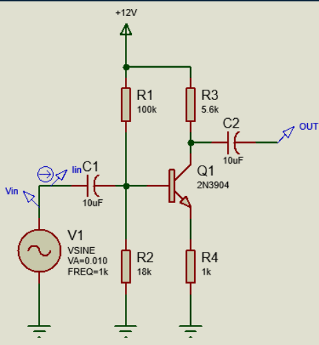
The capacitors C1 and C2 are input and output capacitors used for coupling. The coupling capacitors are used in the amplifier circuit to isolate DC from AC input. The three terminals of the Q1 transistor are:
- the base, connected with R1, R2, and C1.
- the emitter, connected with R4.
- the collector, connected with R3 and C2.
All the resistors R1 to R4 are used for biasing and determining the DC Q-point. The Q-point is used to determine the operating region of the transistor. In this example, the 2N3904 NPN transistor is used in a linear region. The gain of this amplifier is:
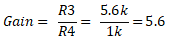
This equation is valid for a single-stage BJT common emitter amplifier only. The gain of an amplifier is usually represented in another unit called decibel (dB). The conversion is followed using this formula:

Where Gain represents the simple gain ratio, which in our case is 5.6. So,
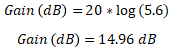
So, the gain of the amplifier given in Figure 1 is 14.96 dB.
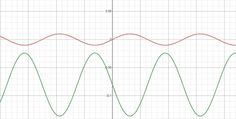
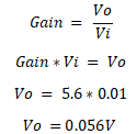
The following figure shows the result of the amplifier circuit. Each unit on the y-axis represents 0.01V. The red waveform (input) is 0.01V, as shown on the graph. The green waveform shows the circuit's output and a voltage of 0.05V from its center, thus an amplified version of the input.
Theoretically, the output should also be:
An important thing to discuss here is the polarity of the output signal. The output is in the opposite direction as the input, which means for every positive peak of the input, we get a negative amplified peak of the output. It is an inbuilt characteristic of the circuit, and thus, the actual gain of the circuit is represented with a negative sign:

An amplifier PCB is a crucial component, and its primary function is to take an input signal from a source and amplify it. Without a well-designed PCB layout, the amplifier circuit may suffer from various issues. Several critical factors need to be considered when designing a PCB layout for amplifier applications, such as:
Capacitor Placement
By placing capacitors close to the relevant pins, the traces connecting capacitors to the other components should be made short. This can help mitigate voltage spikes caused by switching currents.
Power PlaneWhile designing an amplifier PCB, it needs to be ensured that the power planes can meet the circuit's current requirements, especially when multiple ICs share the same power supply plane.
RoutingWhile using a digital signal, especially Class-D outputs and digital signals, careful routing of signals is to be made to minimize interference.
GroundingProper grounding of the PCB is essential to prevent the formation of ground loops. This can be achieved by shorting all unit grounds together.
Best Practices for Amplifier PCB Layout

Similar to the critical considerations in designing amplifier PCBs, there exist essential best practices for optimal amplifier PCB designs:
Crosstalk and NoiseTo mitigate crosstalk, it's critical to ensure that the signals crossing adjacent layers are placed in opposite directions eliminating possibility of parallelism between traces.
Thermal ManagementEffective PCB thermal management involves employing techniques to minimize heat generation during regular operation and mitigate excessive heat buildup under abnormal conditions. Careful selection and distribution of components are essential to ensure that board temperatures are kept at optimal.
Besides, consider using ceramic PCBs with substrate materials like aluminum nitride and aluminum oxide. Ceramic PCBs have excellent thermal dissipation and high-frequency performance, and you don't need to add a heat sink to the amplifier PCB for thermal dissipation anymore.
EMI/EMC Guidelines![]()
PCB designers use diverse strategies to manage electromagnetic interference (EMI) and ensure compliance with electromagnetic compatibility (EMC) standards. The following considerations can be taken into account as EMI and EMC guidelines:
- Adequate separation between traces minimizes the formation of antennas and reduces EMI.
- Maximizing ground plane coverage helps mitigate EMC issues by providing a low-impedance path for returning currents.
- Usage of physical shields enclosing PCBs attenuates radiation by reflecting and absorbing electromagnetic waves.
- Installing decoupling capacitors near the power pins of integrated circuits minimizes noise levels and reduces EMI.
- Employing matched signal termination techniques helps mitigate impedance mismatch in high-speed circuits, reducing EMI-related issues.
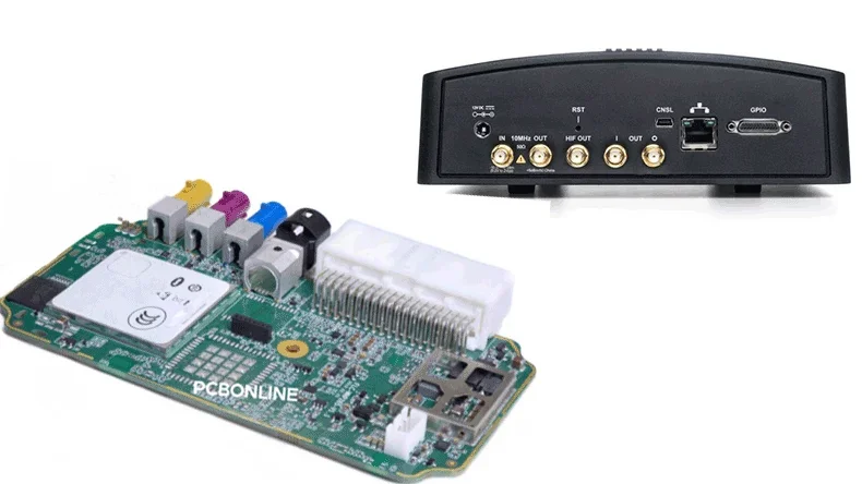
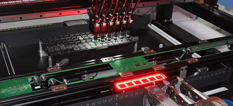
Amplifier PCB and Box-Build Assembly Manufacturing
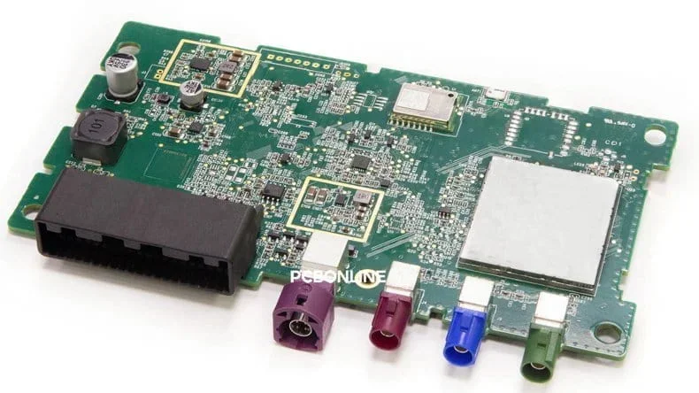
An amplifier is manufactured by fabricating the amplifier PCB, mounting components on the PCB to form a PCBA, fabricating the enclosure, and installing the enclosure to the PCBA to form the final product.
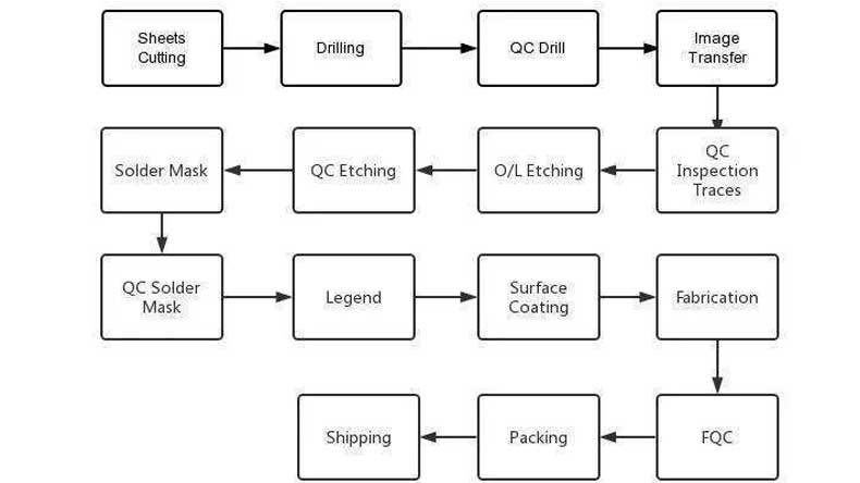
The amplifier PCB fabrication process includes Cut laminate > inner layer circuits > lamination > drilling plating copper > outer layer circuits > pattern plating > etching > solder mask > legend > surface finish > profile > testing > final quality control.
During PCB fabrication, we also source the components and prepare jigs and molds for PCB assembly and testing.
The amplifier PCB assembly process includes Solder mask printing, solder paste inspection >, component placement, X-ray inspection, reflow soldering, and automated optical inspection. If a through-hole component mounting is needed, the assembly process continues, including inserting PTH component leads through holes > and wave soldering.
In the post-assembly stage, we have PCBA value-added services and box-build assembly, including functional testing, thermal aging, IC programming, conformal coating, enclosure manufacturing, and box-build assembly.
You can work with PCBONLINE to turn your amplifier design into real devices. PCBONLINE is a one-stop electronic manufacturing service provider for amplifier applications. We provide all types of PCB fabrication, assembly, component sourcing, PCBA value-added, and box-build assembly until you receive the final products.
Founded in 1999, PCBONLINE has two large advanced PCB manufacturing bases, one EMS PCB assembly factory, and an R&D team that provides one-on-one engineering support and solves technical issues.

PCBONLINE fabricates and assembles amplifier PCBs of many types, including FR4 PCB, ceramic PCB, high-frequency PCB, HDI PCB, etc.
We have powerful manufacturing strength and rich technical experience in thermal management and EMC compliance for amplifier PCBs.
We can manufacture RF amplifier PCBs to have a small impedance tolerance and optimized radio-frequency performances.
You can have amplifier applications manufactured from PCBs and PCBAs to final product box builds from PCBONLINE at one stop, saving you time and costs.
We fabricate and assemble high-quality amplifier PCBs that are certified with ISO 9001:2015, IATF 16949, RoHS, REACH, UL, and IPC-A-610 Class 2/3.
We offer free amplifier samples and PCBA functional testing for bulk production orders.
Whether your amplifier design is for radio frequency applications, sound volume amplify, test instruments, wireless communication, etc, PCBONLINE can work for you on electronic contract manufacturing. If you want to turn your design or initial plan into reality, please get in touch with PCBONLINE by email at info@pcbonline.com.
Conclusion
In summary, amplifiers are pivotal in electronics as they amplify the amplitude of input signals. Thus, understanding amplifier design requirements is crucial for successfully designing, simulating, and manufacturing circuits. Designing an amplifier PCB layout requires attention to various factors to guarantee optimal performance and reliability. To turn your amplifier PCB design into reality, choose PCBONLINE as your one-stop electronic manufacturer.
PCB assembly at PCBONLINE.pdf


