
Impedance control is crucial in printed circuit boards (PCBs), particularly in high-speed and high-frequency PCBs and HDI PCBs. Proper impedance management is essential for signal transmission stability, anti-interference, and power consumption.
In this blog, we will explore the fundamentals of impedance, PCB impedance control, trace width calculations, and design considerations.
Impedance Control
Impedance control in PCBs involves designing signal traces to maintain a specific impedance value within a narrow tolerance range.
We design the PCB trace width and space and stack-up structure according to the required impedance value.
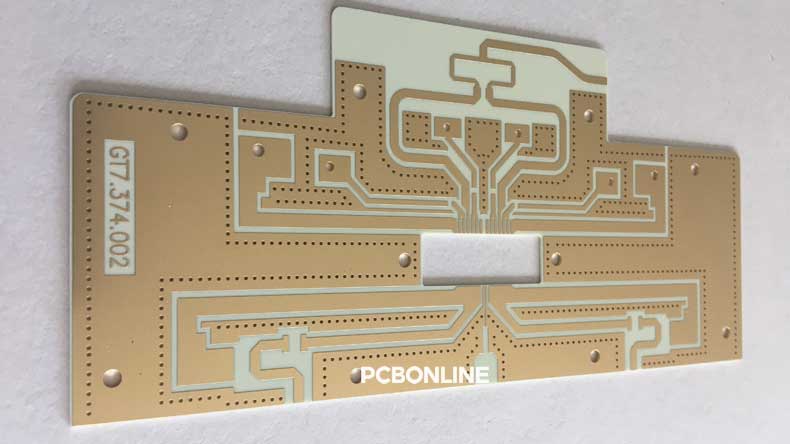
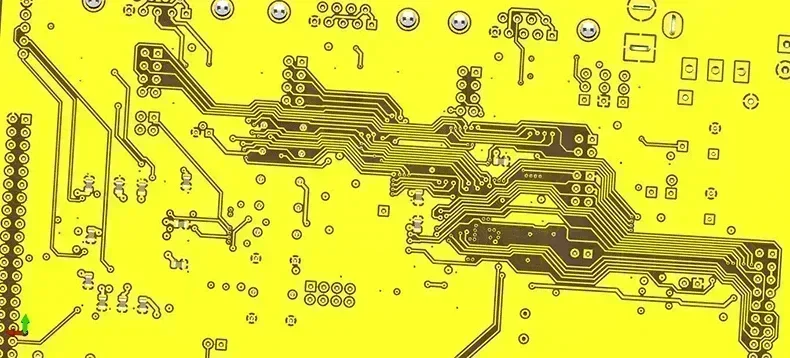
Below are two common impedance control and stack-up designs for 4-layer HDI PCBs by PCBONLINE.
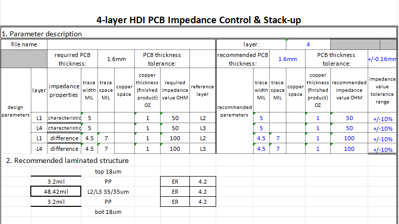
50Ω, 100Ω, thickness 1.6mm 4-layer HDI PCB impedance design V1
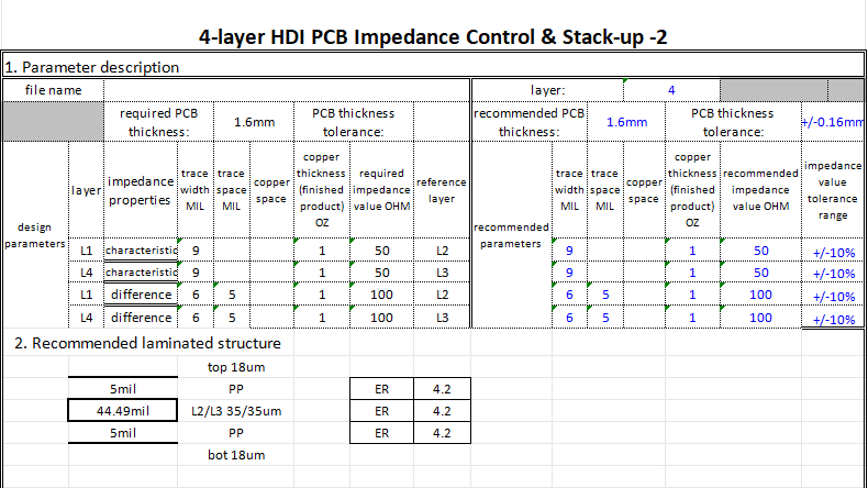
50Ω, 100Ω, thickness 1.6mm 4-layer HDI PCB impedance design V2
This practice is crucial for high-speed digital applications like RF communications, telecommunications, computing (frequencies >100 MHz), and high-frequency analog circuits (e.g., DDR, HDMI, Gigabit Ethernet).
At high frequencies, PCB traces act as transmission lines, where impedance mismatches can cause signal reflections and distortions. Impedance control ensures that the characteristic impedance of the trace matches the source and load, minimizing reflections and preserving signal integrity.
One-Stop PCB Manufacturer and Assembler Dealing with Impedance Control
If your PCB board has requirements for impedance control, the advanced PCB manufacturer PCBONLINE can do the impedance control and provide you with one-stop electronic manufacturing services.
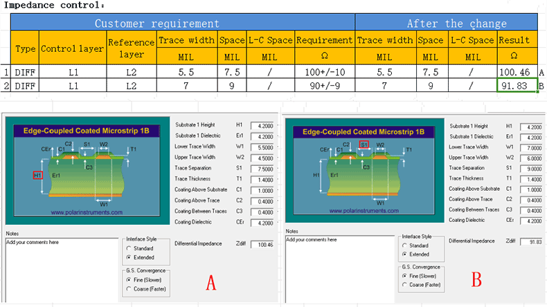
For example, below are two designs for impedance control for a four-layer PCB. PCBONLINE does the impedance control design for the client for free. The impedance control requirements are 100Ω±10% and 90Ω±9%. The impedance results by PCBONLINE are 100.46Ω and 91.83Ω, meeting the client's impedance control requirements.
Whether you have an impedance design or not for your PCB, PCBONLINE can do the impedance control and DFM (design for manufacturing) for your project. Founded in 1999, PCBONLINE has two large advanced PCB manufacturing bases, one PCB assembly factory, stable supply chains, and an R&D team to provide one-stop R&D and PCB assembly.

PCBONLINE can do the impedance design meeting any of your PCB impedance control requirements for free.
Before and during PCBA prototyping, PCBONLINE does DFM, including Gerber and BOM checks, design defect debugging, manufacturing process design, and finding out and solving unexpected issues throughout the entire project to ensure the success of your project.
PCBONLINE has powerful manufacturing and assembly capabilities for HDI PCBs and high-frequency PCBs that require impedance control.
For high-speed and high-frequency PCBs, PCBONLINE has PTFE laminates in stock within a 45-day storage period to ensure the fast delivery and high performance of the PCB boards.
You can order affordable PCB manufacturing and assembly and value-added services from the source factory manufacturer PCBONLINE.
No matter what PCB/PCBA quantity you want, the professionals at PCBONLINE offer one-on-one engineering support throughout your project. To get a quote, please don't hesitate to email info@pcbonline.com.
Why is Impedance Matching Needed?
The primary function of a PCB trace is to transfer signal power from the driver to the receiver. The impedance along the trace must be matched to achieve maximum signal power transfer.
Without impedance matching, high-frequency signals can degrade, causing signal distortion and varying power levels, as seen in distorted eye diagrams. Proper impedance matching ensures that the power from the driver reaches the receiver effectively.
What is Impedance?
Impedance (denoted as Z) measures the opposition to the flow of alternating current (AC) and is a complex quantity comprising resistance (real part) and reactance (imaginary part).
Reactance, which can be inductive or capacitive, provides opposition due to inductance or capacitance:
Inductive Reactance (XL)
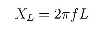
Where f is the frequency (Hz) and L is the inductance (H).
Capacitive Reactance (XC)
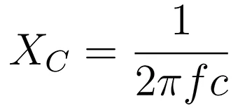
Where f is the frequency (Hz) and C is the capacitance (F).
Factors that Influence Impedance
To achieve effective impedance control, PCB designers must consider several factors:
1. Trace width
- Relationship: Inversely proportional to impedance.
- Control: Controlled via etching processes, ensuring a tolerance of ±10%.
2. Dielectric thickness
- Relationship: Directly proportional to impedance.
- Control: Managed through material selection and lamination processes.
3. Dielectric constant (εr)
- Relationship: Inversely proportional to impedance.
- Control: Different PCB board materials have distinct dielectric constants (e.g., FR4: 3.9–4.5, PTFE: 2.2–3.9).
4. Copper thickness
- Relationship: Inversely proportional to impedance.
- Control: Controlled through pattern electroplating or selecting base material copper foil.
5. Soldermask thickness
- Relationship: Inversely proportional to impedance.
- Control: Controlled through pattern electroplating or selecting base material copper foil.
Calculating PCB Impedance
There's no versatile formula for calculating PCB impedance. Calculating the impedance involves using specific formulas depending on the PCB configuration:
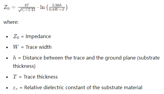
Microstrip Line
PCB impedance formula for a trace on the outer layer with a ground plane below:
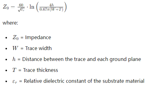
Stripline
PCB impedance formula for a trace embedded between two ground planes:
Due to the complexity of the PCB impedance formulas, you can use simulation software like ANSYS HFSS for detailed impedance calculations based on 3D models. You can also use online calculators like the EEWeb Impedance Calculator for quick estimation.
Determining Trace Width for PCB Impedance Control
The trace width, dielectric height, and material properties define the characteristic impedance of the PCB. The manufacturer specifies parameters like dielectric material, its relative permittivity, and the height between layers, usually aiming for standard impedance values like 50 or 75 ohms.
For the desired impedance, trace width is calculated using tools like free impedance calculators. For example, for a 50-ohm impedance with a dielectric height of 0.2 mm and a relative permittivity of 4.6, the required trace width is about 0.3 mm.
Once the trace width is determined, it is implemented in PCB design tools like KiCad. For instance, in a GPS receiver project requiring a 50-ohm matched antenna input, all traces from the receiver to the SMA connector must be matched to 50 ohms. A ground plane on the first inner layer aids in impedance matching. Setting the trace width to 0.3 mm in the design tool and ensuring proper ground plane setup enables successful routing of impedance-controlled traces.
Conclusion
Controlled impedance design is manageable with an understanding of the principles and appropriate calculation tools. Ensuring a good match within acceptable tolerances guarantees reliable performance in RF and high-frequency circuits. If your PCB needs impedance control, work with PCBONLINE which offers free impedance design and DFM and one-stop electronics manufacturing.
PCB fabrication at PCBONLINE.pdf


