
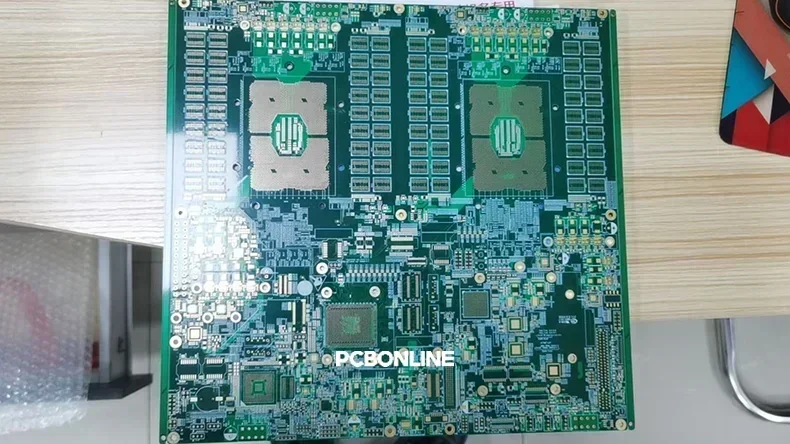
AI, IoT, and high-speed computing drive their electronic hardware to run powerful functions with a high circuit density, which requires the HDI (High-Density Interconnect) technology on the PCB (printed circuit board). At PCBONLINE, we specialize in HDI PCB fabrication and assembly to build the AI servers, AIoT, wearables, communication, automotive, and consumer electronic devices.
Explore what PCB HDI means, via structures, stack-ups, and the industry-leading HDI PCB manufacturing capabilities we offer.
What does HDI mean for PCBs?
An HDI PCB is a printed circuit board with a higher wiring density per unit area than a conventional board. Defined by the IPC-2226 standard, HDI PCBs use laser-drilled holes (≤150μm in diameter) and sequential lamination to create complex blind and buried via structures.
By using microvias, thinner materials, and tighter trace/space, HDI allows for more components to be placed on both sides of the PCB, reducing size and weight while enhancing signal integrity.
If the microvias stack, they form a stacked via; if staggered, they form a staggered via. Stacking microvias is more complex, therefore, more expensive.

At PCBONLINE, the HDI PCB stackup we support is 1+N+1 to 4+N+4 and any-layer interconnect. Sequential lamination is related to the HDI stackup.
A standard multilayer core is the "N", which is laminated, through-hole drilled (blind via), plated with copper, and then filled with resin to make the blind vias flat.
Sequential lamination is adding a layer of prepreg and copper foil on both sides of the finished core, laminating, laser drilling the outer layers (laser only penetrates a layer of copper foil to make the microvia), plating the microvias, and imaging and etching the circuit pattern on the new outer layers. This is the first cycle. Repeating this process, it is a 2+N+2 structure.
For higher structures, the above process repeats 2 through 4 or even 5 for the next set of layers.
The Core of HDI PCB: Microvia
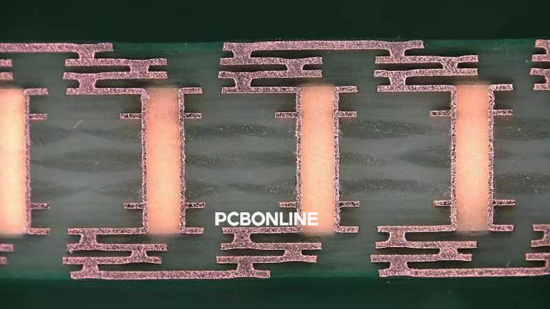
The secret to high density lies in the PCB microvias. Microvias are laser-drilled holes ≤0.15mm (150μm) that connect adjacent layers.
As mentioned, microvias form stacked and staggered vias. Stacked vias are microvias placed directly on top of each other, saving space but requiring precision copper filling. Staggered vias are offset between layers.
In an HDI PCB, you must understand microvias. The below important terms are related to the HDI PCB's microvia, and you can find what capabilities PCBONLINE can provide.
Laser hole diameter is the physical size of the hole created by a laser beam (CO2 or UV laser). At PCBONLINE, the maximum laser hole diameter is 0.25mm, and the minimum is 0.1mm.

The aspect ratio is the ratio between the depth of the microvia and its diameter. If the microvia is too deep and narrow, the plating chemicals cannot circulate effectively. At PCBONLINE, the maximum aspect ratio of the laser hole is 1:1 (depth including copper thickness).

Plated copper filling (copper shut) is the process of completely filling the laser-drilled microvia with solid electroplated copper during the plating cycle. Unlike through-holes that are only "walled" with copper, HDI microvias are often filled "shut" to create a solid copper pillar. At PCBONLINE, we can do this process, and our laser via is in the size of 0.1mm to 0.125mm (priority 0.1mm).
This is mandatory for stacked vias. It provides the best electrical and thermal conductivity and creates a flat surface for the next layer of lamination or for soldering a component directly on top (via-in-pad).

Via filling with resin involves plugging a microvia with a non-conductive epoxy resin, which is then baked, cured, and planarized (sanded flat). While microvias are usually copper-filled, buried vias (the larger holes in the inner core) are typically filled with resin.
Resin filling prevents air bubbles from being trapped during the next lamination cycle and prevents solder from "wicking" into the hole during PCB assembly. It is a more cost-effective way to achieve a flat surface compared to using pure copper. At PCBONLINE, we can do this process.

HDI Stack-up: From 1+N+1 to 4+N+4 and Any-Layer
The HDI structure of an HDI PCB is defined by the number of laser-drilled layers. At PCBONLINE, our manufacturing expertise covers the full spectrum of complexity.
1+N+1 & 2+N+2 are the standards for most consumer electronics.

3+N+3 & 4+N+4 are advanced structures for AI servers and medical equipment.

Any-layer interconnect means any two layers can be connected by stacked microvias, offering maximum design flexibility for ultra-compact devices like smartphones.

What Else of PCBONLINE's HDI PCB Capabilities
To ensure the reliability of your high-speed designs, PCBONLINE adheres to rigorous manufacturing tolerances. Besides the above microvia capabilities and HDI structures from 1+N+1 to 4+N+4 and any-layer-interconnect, below are all what things we can do in HDI PCBs.
Our advanced laser drilling technology ensures extreme accuracy in hole placement.
The space between laser hole edges in the same net prevents signal interference. At PCBONLINE, the minimum space between laser hole edge to laser hole edge in the same net is 0.1mm.

The pace between laser hole edges in different nets is for high-voltage insulation and reliability. At PCBONLINE, the minimum space between the laser hole edges in different nets is 0.25mm.

The space between the laser hole in the outer layer and the buried hole edge in the same net ensures structural integrity and reliability of the connection. At PCBONLINE, the minimum space between the laser hole edges in the Same Net is 0.15mm.

The space between the laser hole wall edge and the buried drill hole wall edge in different nets ensures electrical isolation and prevents conductive anodic filament growth between the microvia and the core's buried via. At PCBONLINE, the minimum space between the laser hole wall edge and the buried drill hole wall edge in different nets is 0.3mm.

The space between the laser hole center and PCB edge (inner layer) ensures the laser hole doesn't end up too close to the edge of the PCB, preventing delamination or exposed copper after the PCB is cut. At PCBONLINE, the minimum space between the laser hole center and PCB edge (inner layer) is 0.4mm.

The space between the laser hole center and PCB stamped/routed edge (outer layer) ensures that, when depaneling, the mechanical stresses of the router bit do not crack the fragile copper plating inside the laser hole. At PCBONLINE, the minimum space between the laser hole center and PCB stamped/routed edge (outer layer) is 0.35mm.

The space between the PTH hole edge and the Pad (Outer layer) in different nets ensures no solder bridge in the PCB assembly process. At PCBONLINE, the minimum space between the PTH hole edge and Pad (Outer layer) in different nets is 0.2mm.

Partner with HDI PCB Manufacturer PCBONLINE for AI Hardware and High-Speed Computing
PCBONLINE is an OEM HDI PCB manufacturer providing turnkey HDI PCB manufacturing for AI applications. With 70–80% of PCBs for AI hardware produced in China, PCBONLINE stands out as a trusted HDI PCB manufacturer. We offer 24+ layer GPU HDI PCBs, turnkey PCBA, and OEM services.

Founded in 2005, PBONLINE has two large advanced PCB manufacturing bases and one PCB assembly factory.
AI HDI PCB fabrication with HDI via-in-pad copper filling for GPU designs with 24+ layers.
We provide one-stop AI HDI PCB manufacturing, including component sourcing, PCB fabrication, assembly, testing, and system integration.
SMT assembly with fine-pitch BGA placement accuracy and custom reflow profiles for warpage-free soldering.
100% X-Ray inspection, functional testing, and burn-in testing for guaranteed reliability.
We have rich experience in impedance control, oven temperature control, and assembly fixture designs.
Our vacuum-controlled plating lines ensure void-free copper filling for stacked vias.
High-quality HDI PCBA manufacturing certified with ISO 9001:2015, ISO 14001:2015, IATF 16949:2016, RoHS, REACH, UL, and IPC-A-610 Class 2/3.
At PCBONLINE, we can help our clients reduce costs while achieving the highest levels of performance and reliability. If you feel interested in HDI PCBs from PCBONLINE, send your inquiry by email to info@pcbonline.com.
Conclusion
HDI PCBs use microvias with the sequential lamination technology. From AI servers and accelerators to networking, AIoT, high-speed computing, communication, and medical electronics, PCBONLINE provides turnkey HDI PCB manufacturing. If you are looking for a trusted partner for HDI PCBs, contact the HDI PCB manufacturer PCBONLINE for OEM manufacturing.
PCB assembly at PCBONLINE.pdf


