
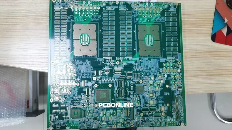
Artificial Intelligence (AI) is reshaping industries worldwide, from cloud computing and robotics to AI servers and medical long-term care. HDI PCB (high-density-interconnected printed circuit board), with 24+ layers, is the foundation that supports and connects all electronic components of AI devices. The critical components mounted on an AI HDI PCB include GPU, CPU, DRAM, PCIe, and a voltage regulator module.
PCBONLINE, an OEM HDI PCB manufacturer, provides HDI PCB fabrication and turnkey PCB assembly for AI devices. With in-house factories, advanced production equipment, and strict quality systems, PCBONLINE delivers reliable and high-performance AI HDI PCBs to clients around the globe.
HDI PCBs for AI Hardware Building
AI servers and accelerators rely on GPUs, CPUs, and sometimes FPGAs, each with thousands of I/O connections in dense BGA packages. To route these signals while maintaining signal integrity, low loss, and thermal stability, only HDI multilayer PCBs can meet the requirements.
- 24+ PCB layers: High-end GPU PCBs typically have 24–60 layers, with stacked vias and blind/buried interconnections.
- Inner-layer routing: High-speed GPU-to-memory signals are routed on inner layers to shield them from EMI.
- High power delivery: GPUs draw hundreds of watts. Wide copper planes, busbars, and power distribution layers are integrated.
- Thermal management: Thick copper, thermal vias, and high-Tg laminates prevent overheating under 24/7 workloads.
Among the HDI PCBs for AI, AI server PCBs are considered the pinnacle of PCB technology, whose manufacturing requires precision and experience.
China's Leadership in AI Server PCB Manufacturing
China is a global leader in HDI PCB production for AI electronics hardware building. 70%–80% of AI server PCBs worldwide are manufactured in China. PCBONLINE stands out as an HDI OEM PCB manufacturer for AI devices. Our AI HDI PCB dominance comes from:
- Mature and independent HDI PCB fabrication processes
- Advanced local supply chains for materials and components like BGAs and FPGAs
- Strong OEM/ODM capabilities, ensuring both quality and scale
PCBONLINE is a mid-to-high-end HDI PCB manufacturer for AI devices, industrial electronics, automotive systems, and medical equipment.
PCBONLINE's HDI PCB Manufacturing Process
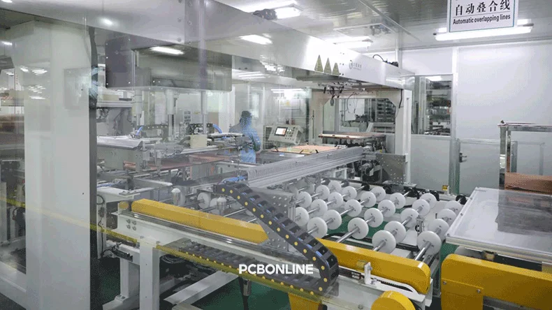
At PCBONLINE's factories, we manufacture HDI PCBs for AI devices through a highly controlled process with advanced automation.
Key steps from our HDI PCB manufacturing include —
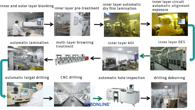
Inner layer processing:
At PCBONLINE's factories, the process begins with inner layer preparation. Copper-clad laminates are cut and cleaned before dry film is laminated. Using laser direct imaging (LDI), inner-layer circuitry is exposed with sub-micron precision, followed by developing, etching, and stripping. After that, each inner layer is inspected by automated optical inspection (AOI) to ensure zero defects before multilayer bonding.
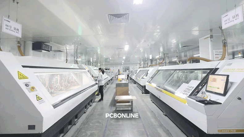
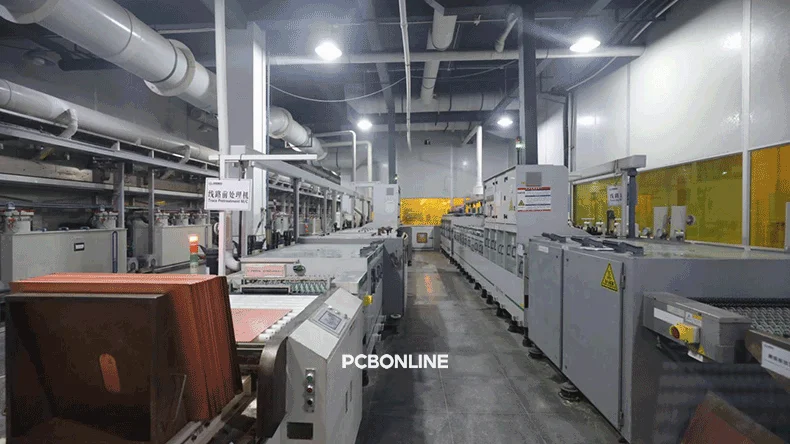
Drilling and plating:
Next comes PCB via drilling and plating. High-speed CNC machines drill through-holes, while CO₂ and UV lasers create microvias essential for HDI interconnections. The drilled holes are deburred and desmeared, then sent through plasma and chemical treatment lines. With plated through-hole (PTH) processes and vertical continuous plating (VCP) lines, copper is deposited evenly inside microvias and through-holes, guaranteeing strong interlayer connections.
Multilayer lamination:
Once the inner layers and vias are prepared, the PCB undergoes multilayer lamination. Automated presses align and bond the stack of cores, prepregs, and copper foils under heat and pressure. Alignment targets and X-ray registration systems guarantee that the 24+ layers stack up perfectly without misregistration.
Outer layer processing:
After lamination, the outer layers are processed much like the inner layers, with LDI exposure, developing, and etching to define traces as fine as 40–50 microns.
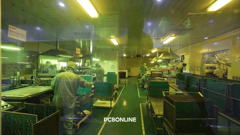
Solder mask and silkscreen:
Solder mask application follows, where the PCB is coated with photoimageable epoxy and aligned by CCD-guided exposure systems to ensure precise pad openings. Silkscreen printing adds identifiers and component markings. For AI server PCBs, the most common surface finish is ENIG (Electroless Nickel Immersion Gold), which provides flat, oxidation-resistant pads suitable for fine-pitch GPU BGAs.
Testing and quality assurance:
After fabrication, every PCB undergoes extensive testing and inspection. Automated optical inspection (AOI) checks for etching defects, while flying probe and four-wire testers verify electrical continuity and impedance. X-ray inspection confirms BGA pad alignment and via quality inside multilayer stacks. Environmental and reliability tests, such as thermal cycling, ionic contamination checks, RoHS/REACH compliance, and impedance measurements, validate that each PCB meets IPC Class 3 standards.
This detailed process, from inner-layer imaging to final reliability testing, ensures that our HDI PCBs for AI devices meet IPC Class 3 standards for high-reliability AI hardware.
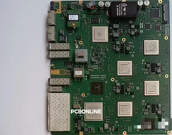
AI Applications Using HDI PCBs

HDI PCBs from PCBONLINE power a wide range of AI-driven devices:
- AI servers: High-density GPU PCBs with 24–30 layers, supporting PCIe Gen5, NVLink, and DDR5 memory channels for cloud and enterprise computing.
- AI accelerators: Custom FPGA or GPU accelerator cards for deep learning, scientific computing, and rendering, often with integrated high-bandwidth memory (HBM).
- Networking and storage servers: HDI PCBs enabling 100G/400G Ethernet, InfiniBand, and high-throughput storage systems with strict impedance control.
- Edge AI devices and robotics: Compact HDI PCBs combining AI processors, wireless communication modules, and sensors for drones, robots, and autonomous vehicles.
- Medical and automotive AI: High-reliability HDI PCBs for imaging systems, autonomous driving controllers, and advanced driver assistance systems (ADAS).
Partner with HDI PCB Manufacturer PCBONLINE for AI Hardware Building
PCBONLINE is an OEM supplier providing turnkey PCB manufacturing for AI applications. With 70–80% of PCBs for AI hardware produced in China, PCBONLINE stands out as a trusted HDI PCB manufacturer. We offer 24+ layer GPU HDI PCBs, turnkey PCBA, and OEM services.

Founded in 2005, PBONLINE has two large advanced PCB manufacturing bases and one PCB assembly factory.
AI HDI PCB fabrication with HDI via-in-pad copper filling for GPU designs with 24+ layers.
We provide one-stop AI HDI PCB manufacturing, including component sourcing, PCB fabrication, assembly, testing, and system integration.
SMT assembly with fine-pitch BGA placement accuracy and custom reflow profiles for warpage-free soldering.
100% X-Ray inspection, functional testing, and burn-in testing for guaranteed reliability.
We have rich experience in impedance control, oven temperature control, and assembly fixture designs.
Supporting IC programming in the Cloud way, manipulated by you, and protecting your intellectual property.
High-quality HDI PCBA manufacturing certified with ISO 9001:2015, ISO 14001:2015, IATF 16949:2016, RoHS, REACH, UL, and IPC-A-610 Class 2/3.
At PCBONLINE, we can help our clients reduce costs while achieving the highest levels of performance and reliability. If you feel interested in AI HDI PCBs from PCBONLINE, send your inquiry by email to info@pcbonline.com.
Conclusion
HDI PCBs enable GPUs, CPUs, and accelerators to deliver massive computing power. From AI servers and accelerators to networking, robotics, and medical electronics, PCBONLINE provides turnkey HDI PCB manufacturing for AI hardware. If you are looking for a trusted partner for AI HDI PCBs, contact the HDI PCB manufacturer PCBONLINE for OEM manufacturing.
PCB assembly at PCBONLINE.pdf


