
Applications from industrial systems to our daily life electronics heavily rely on digital circuits. The digital circuits are based on microcontrollers and processors. From the microcontrollers in smartwatches to the powerful processors in data centers, digital circuits enable the fast, reliable, efficient, and secure processing of information. Designing the digital circuits specifically on the printed circuit boards (PCBs) needs more precision, accuracy, impedance matching, and understanding of EMC and EMI challenges. In the context of digital circuits and PCBs, we'll dive deep into the challenges faced and how to mitigate them.
In this article:
Part 1: Overview of Digital Circuits Part 2: Digital Circuits High-Speed Pulse Signals (Square Waves) Part 3: What to Take Care of in Digital Circuit Design? Reducing EMI Part 4: PCBs Mainly Based on Digital Circuits Choose PCBONLINE for Digital-Circuit PCB ManufacturingOverview of Digital Circuits
When we say digital, the first thing that comes to our minds is that we are talking about discrete signals (numbers), binary states represented as combinations of 0s and 1s (low and high voltages).
Unlike analog circuits, which handle continuous signals (every possible state between low and high voltage), digital circuits use logic gates (AND, OR, NOT, XOR, etc.) to handle data and perform operations like computation, data storage, and signal processing.
These form the basis of digital devices like RAMs, NOR/NAND Flash, microcontrollers, microprocessors, and FPGAs. The digital systems vary from simple to complex ones, like latches and flip-flops, to Single Board Computers (SBCs) and CPUs with millions of transistors working and switching at a time, causing noise and heat.
Digital Circuits High-Speed Pulse Signals (Square Waves)
The digital signals/data are travelling at a few to many MHz of frequency in the form of pulses (square waves), switching rapidly between low and high states. While it enables fast transmission of data, the fast and sharp transitions also create challenges with electromagnetic interference (EMI). These high-speed signals require advanced techniques in PCBs to overcome the EMI/EMC effects, and the PCBs to perform as expected.
Many digital circuits require clocks to operate and synchronize their functions. Communication protocols, for example, need common clocks to ensure accurate data exchange between different circuit parts. These clocks and the data buses are major sources of EMI.
What to Take Care of in Digital Circuit Design? Reducing EMI
Besides digital circuits, PCB design can also involve analog, RF, microwave, and power circuits. PCB design with mixed circuits requires careful planning for mitigating EMI issues to ensure reliable operation for which the board is meant to be designed. The switching creates noise and crosstalk among different parts of the circuit, rendering the performance and functionality of the PCB.
The art of mitigating EMI issues from the PCB requires special considerations and steps to be taken:
The first thing in designing a good electromagnetic compatibility EMC PCB is to define a good layer stack-up with a combination of signal and ground layers.

The second is to choose the appropriate material for the PCB. Depending upon the type/application of PCB, you can choose whether to go for FR-4 or Rogers, etc.
Designing a high-speed PCB comes with optimization of price and performance, so choose wisely.
Define the separate areas for digital, analog, RF and microwave, and power circuits on the PCB.
Keep the analog and digital grounds separate and make them common on the plane layers through stitching vias to minimize ground noise.
Always keep the return path as close to the signal track as possible to reduce the loop areas; this will reduce EMI effects.
Use ground planes to provide low-impedance return paths to high-speed signals.
Perform impedance matching for differential pairs and RF circuits. Typically, high-speed signals like USB, HDMI, and DDR are matched to 90-100Ω. RF tracks require special techniques based on stripline and microstrip transmission lines for impedance matching to 50Ω.
A good practice is to add series/parallel termination resistors, which make impedance matching easy and help avoid signal reflections.
Don't allow net antennas on the PCB by setting the DRC rules in the CAD software like Altium Designer, etc.
Use decoupling capacitors to stabilize the power rails and place them near the power pins so that ICs get a filtered supply.
RF and microwave circuits need special shielding techniques to keep them intact from external and internal interference. This shielding can be done by placing metal cages/boxes around them and also by designing matching networks and impedance matching.
Keep the RF ground separate as well.
Fence the impedance matched tracks through vias and grounded copper pours.
Don't allow impedance discontinuities to avoid harmonics in the high-speed and RF tracks. This can be done by keeping the track's length as short as possible and by good matching.
Good Design Practices: For designing a working PCB, you have to keep these things in mind.
- Choose the layer stackup in coordination with the PCB manufacturer so that the PCB is manufacturable.
- Design a PCB that is easy to probe by placing test-points, so you can test and validate it, but remember it should not be at the cost of performance.
- PCB should comply with DFM (Design for Manufacturing) and DFA (Design for Assembly).
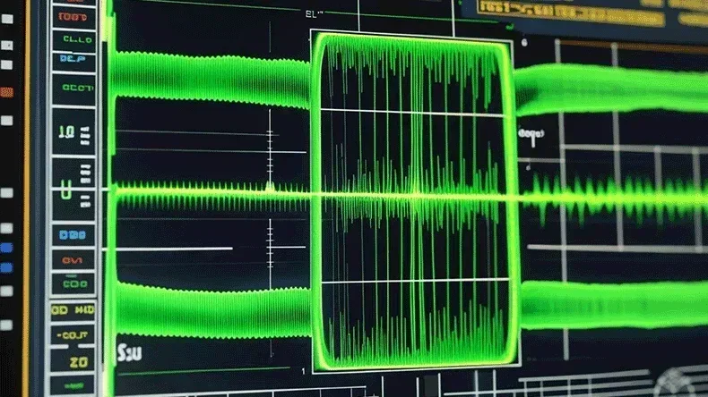
- Use SPICE tools like Cadence, ADS to simulate the signal integrity and eye diagrams to ensure impedance matching.
PCBs Mainly Based on Digital Circuits
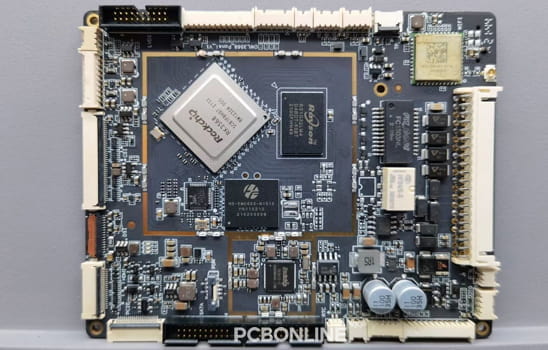
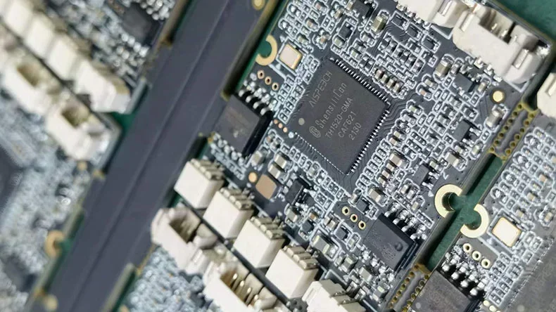
The digital-circuits PCBs are typically used in applications that require high-speed processing, such as those based on microcontrollers (e.g., STM32, ESP32), FPGAs, or ARM-based chips. These boards are used in embedded systems and high-performance computing platforms. Below, I'll summarize the key features of digital circuit-based PCBs:
Frequent signal changes
Digital circuits are based on transistors, which operate at switching speeds in MHz or GHz frequencies. This switching causes electrical noise and raises the device's noise figure, making other signals prone to noise and hence degrading performance. This requires careful design to manage signal integrity and minimize EMI.
Complex clock signal network
These PCBs include clock signals to synchronize different ICs for their correct operation. These clock signals require precise routing and termination as discussed earlier.
High-density wiring
High-speed and high-density interconnect (HDI) PCBs run digital circuits. The FPGAs and ARM-based chips have a high number of I/O pins and complex interconnects. These interconnects are high-speed and route from one end of the PCB to the other. These tracks demand careful routing to mitigate crosstalk, signal degradation, and signal integrity.
Strict impedance control requirements
High-speed interfaces like DDR, USB, HDMI, and PCIe transfer data at MHz speeds and require controlled impedance traces to ensure reliable data transfer.
Complete ground plane
A continuous ground plane is critical to provide a low-impedance return path, reduce signal reflections and EMI, and improve signal integrity. PCBs based on high-speed digital circuits often require dedicated ground layers.
Obvious module partition design
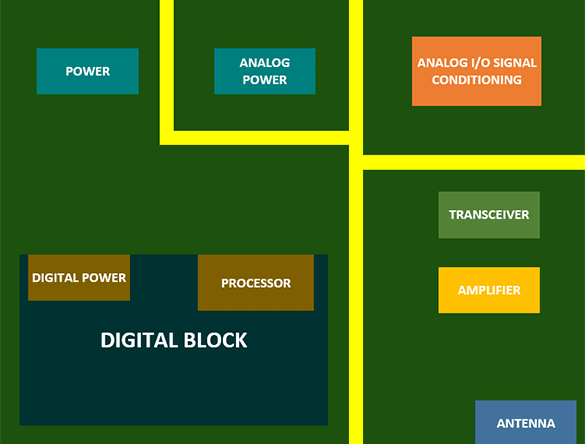
High-speed HDI PCBs are often partitioned into functional blocks (e.g., power, processing, memory, I/O, RF, and analog). They are kept separate to reduce EMI.
4 to 6 layers and above
High-density wiring requires multilayer PCBs to accommodate traces well and for controlling impedance, and providing dedicated ground planes. Digital PCBs typically use 4, 6, or more layers. For example, an FPGA or ARM-based PCB might use 8 layers to handle complex routing.
PCB design heavily relies on auto-wiring
Due to their complex and high-density wiring, digital circuit PCBs are often auto-routed to optimize trace layouts and reduce human efforts, though manual adjustments and impedance matching are still needed for critical signals like data and clocks.
Choose PCBONLINE for Digital-Circuit PCB Manufacturing
When it comes to manufacturing PCBs for digital circuits, partnering with a reliable turnkey PCB manufacturer like PCBONLINE can streamline the process. PCBONLINE provides PCB fabrication and assembly for digital-circuit PCBs. One-on-one engineering support and professional DFM are available all the way.

Founded in 1999, PCBONLINE has two large advanced PCB manufacturing bases, one turnkey PCB assembly factory for PCB assembly and box-build assembly, stable material supply chains and strategic cooperation with electronic component manufacturers, and long-term cooperation with the top 3 mold and enclosure manufacturers in China for jigs/fixtures, molds, and enclosures.
Besides, PCBONLINE has an R&D team and professional CAM engineers for project development and DFM, which ensures the reliability of your PCB grounds.
Our one-on-one engineering support ensures your design is optimized from the start, while the professional DFM services help catch potential issues early, reducing costly revisions.
The R&D team of PCBONLINE can complete or take part in the development of your project, including PCB grounding.
One-stop OEM manufacturing for digital circuits, from PCB fabrication, component sourcing, and PCB assembly to IC programming, box-build assembly, and value-added services.
Provide various types of PCBs for digital circuits, such as high-speed/high-frequency PCBs, HDI PCBs, multilayer PCBs, and ceramic PCBs.
Whether you're building an STM32-based device, an ARM-chip-based module, or an FPGA-based compute platform, PCBONLINE's expertise ensures high-quality boards that meet strict performance and reliability standards.
High-quality PCB and PCBA manufacturing certified with ISO 9001:2015, ISO 14001:2015, IATF 16949:2016, RoHS, REACH, UL, IPC-A-600 Class 2/3, and IPC-A-610 Class 2/3.
When your project goes to the massive production stage, PCBONLINE refunds the fees of prototyping, components of the prototypes, R&D, and offers free PCBA functional testing.
Partnering with a trusted OEM PCB manufacturer like PCBONLINE ensures that your intricate designs built around microcontrollers like STM32, ESP32, or ARM-based chips are brought to life with high-quality fabrication, assembly, and professional DFM support. To get a quote for your project from the turnkey PCB manufacturer PCBONLINE, contact info@pcbonline.com.
Conclusion
Digital circuits are the backbone of modern electronics, powering a vast array of devices. Their reliance on high-speed, binary signals enables fast and efficient processing, but it also introduces challenges like EMI, signal integrity, and complex routing when designed on PCBs. By carefully addressing these challenges through proper layer stackup, impedance matching through dedicated ground planes, and module partitioning, designers can create reliable, high-performance digital circuit-based PCBs.
Digital-circuit PCBs feature high-density wiring, complex clocking networks, and multi-layer PCBs, demanding precision in both design and manufacturing. To drive innovation and deliver cutting-edge electronic solutions, you can partner with the turnkey PCB manufacturer PCBONLINE for professional DFM and reliable PCB manufacturing and assembly.
PCB fabrication at PCBONLINE.pdf


