
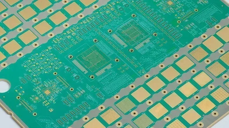
Are you working on high-speed and high-frequency PCB (printed circuit board) projects and struggling with the balance of RF performance and your tight budget? We can help you build cost-effective high-frequency PCBs. Recently, our PCBONLINE team received a client request to build a 100Ω impedance low-cost high-frequency PCB assembly using laminate material with a low Dk of 3 to 3.5. We designed the 6-layer PCB stackup and provided OEM PCB manufacturing, meeting their requirements. In this article, we will use this showcase to show you how PCBONLINE offers a one-stop solution for affordable and high-performance RF and high-frequency PCBs.
Design Requirements and Cost of Our 6-Layer High-Frequency PCB
Our client requested the high-frequency PCB to be an HDI PCB with blind vias, in the size of 50mm x 42.62mm, 1.67mm thick, 6-layer (false 8-layey), inner and outer copper layer of 1oz, surface finishes of immersion gold 2u'' + edge connectors 16u'', impedance of 100Ω, using laminate material with a low Dk of 3 to 3.5.
Our engineers meet these requirements easily. However, the above specification information is not complete. We added the green solder mask + white legend, the PCB panelization of 1 panel containing 2 PCBs with 2mm x 5mm edge rails + 2mm spacing (inverted panelization), trace width/space of 4mil/mil.
What about the high-frequency laminate used for this RF PCB? Our client required "cheap" high-frequency PCBs but wanted to use Rogers RO4350B with the Dk of 3.48. However, the Rogers RO4350B laminate cost for 5 PCBs is $1630.
So how did PCBONLINE manage to make the high-frequency PCB laminate affordable? Our engineers suggested that our client use Taizhou Wangling CT350 with the Dk 3.5 rather than Rogers RO4350B.
By changing the option of the high-frequency PCB laminate, we lowered the laminate cost to $1180 for 5 pieces of 6-layer HDI high-frequency PCBs.
For this high-frequency PCBA small-batch OEM project, we quoted $2130, including the 5 pieces of the 6-layer HDI high-frequency PCB, electronic components, and PCB assembly.
Our High-frequency PCB Solution: Differentiated Stackup Design
High-frequency PCB design typically is a differentiated stackup design, which means a hybrid copper foil stack-up. The showcase PCB in this article is also such s stackup design as follows. It features hybrid copper foil and prepreg (PP) types.

Hybrid copper foil
Among its 6 circuit layers, the outer Layers 1 and 6 use copper foil CF-008, while the inner Layers 2 to 5 use copper foil CF-009. What purpose of using different copper foil types in high-frequency layers?
Outer layers (1 & 6) use CF-008 to enhance adhesion and soldering reliability. Outer layers bear pads, plating, solder coating (HASL/ENIG), gold fingers, and are exposed to mechanical stress and thermal impact during soldering. So they must have strong adhesion to the dielectric layer and higher surface roughness to enhance bonding strength.
Inner layers (2–5) use CF-009 to optimize signal transmission, reduce insertion loss, and minimize reflection. Inner layers contain high-speed signal traces, such as differential pairs, clock lines, and RF lines, and power and ground planes. The smoother the copper surface, the lower the signal loss. CF-009 has a Low Profile, minimizing signal attenuation and improving impedance control.
Different PP types
Besides the hybrid copper foil, the example high-frequency PCB in this article uses different prepreg (PP) for comprehensive optimization of dielectric constant, thickness, loss, and processability.
In this high-frequency PCB, the PP layers between circuit Layers 1-2 and 5-6 use PP-026, which is thicker with a higher Dk. They provide mechanical support and outer-layer lamination buffering, which also helps absorb thermal stress.
The PP layers between circuit layers 2-3 and 4-5 use PP-027, which is thinner with a low Dk and low Df. They provide dielectric isolation between signal layers, ensuring impedance control and low signal loss.
The hybrid copper foil stackup is not only the showcase PCB in this article, but is commonly used in high-speed and high-frequency PCBs and multilayer controlled impedance designs such as HDI PCBs. Applications such as communication boards and GPU AI server motherboards use PCBs with a differentiated stackup design.
HDI Design in High-frequency PCBs

In our showcase 6-layer high-frequency hybrid HDI PCB, you can find that this PCB has through-vias (L1–L6) and mixed-depth laser microvias: short blind vias L1→L2 & L5→L6, and two-layer blind vias L1→L3 & L4→L6. Its design is a multi-step lamination HDI design that requires a sequential build-up process.
In high-frequency and high-speed PCBs, it is common to use an HDI design. This is because HDI structures align with the signal integrity requirements of high-frequency transmission from three respects:
- Shorter signal paths and fewer vias: HDI PCBs use micro-blind and buried vias, which reduce the number of layers a signal must traverse. At high frequencies (>1 GHz), any excessively long path or reflection can cause signal loss or crosstalk. Micro-blind vias can directly connect adjacent signal layers without going through the entire board.
- More uniform impedance control: High-frequency PCBs require strict impedance control. An HDI design features thin dielectric layers, uniform copper thickness, and high-precision laser via positioning, contributing to stable impedance.
- Reduced parasitic inductance and capacitance: Shorter blind/buried vias of an HDI design lead to lower parasitic inductance, and its thin dielectric means a lower parasitic capacitance. This reduces signal attenuation in high-frequency traces, making an HDI design ideal for antennas, filters, RF front-ends, SerDes differential links, etc.
Common high-frequency HDI stackups include:
|
HDI structure
|
Feature
|
High-frequency applications
|
|
1+N+1
|
Single-level HDI (outer-layer blind vias)
|
High-frequency communication modules, antenna matching circuits
|
|
2+N+2
|
Two-level HDI (multi-layer blind vias)
|
High-speed digital / RF mixed boards
|
|
3+N+3
|
Three-level HDI (stacked blind vias)
|
High-end routers, RF base station main boards
|
|
Any-layer HDI
|
Interconnects at any layer
|
High-frequency AI compute boards, millimeter-wave radar mainboards
|
Order Cost-Effective High-Frequency PCBs from PCBONLINE at One Stop
If you have a project plan for high-speed or high-frequency applications, whether you have completed the high-frequency PCB design or not, you can work with the one-stop advanced PCB manufacturer PCBONLINE for affordable and high-quality RF PCB manufacturing and assembly.

Founded in 2005, PCBONLINE has two large advanced PCB manufacturing bases, one PCB assembly factory, stable supply chains, and an R&D team.
Provide one-stop high-speed and high-frequency PCB manufacturing, including R&D, prototyping, PCB fabrication, component sourcing, PCB assembly, PCBA value-added, and box-build assembly.
Minimum laser drill: 0.075mm, minimum mechanical drill: 0.15mm, with microvia structures of 100 µm and 125 µm. High-density circuit layers up to 20, and microvia layers up to 64.
PCBONLINE grasps the core technologies for high-frequency PCB manufacturing, such as impedance control, embedded antenna DFM, expansion/contraction control, etc.
Have ready-to-use high-speed PCB base materials in stock, and the storage period is within 45 days (at manufacturers who have no storage, it usually takes 2 to 3 months to purchase base materials).
Can make various hybrid high-frequency PCBs, including Rogers FR4 PCB and Rogers FR4 ceramic PCB.
High-quality high-speed/high-frequency PCB manufacturing certified with ISO 9001:2015, ISO 14001:2015, IATF 16949:2016, RoHS, REACH, UL, and IPC-A-600 Class 2/3.
PCBONLINE pays attention to quality and cost-effectiveness in high-speed high-frequency PCBs. If you want to get a quote or ask questions about Rogers FR4 PCBs, you can send emails to info@pcbonline.com to get a quote.
Conclusion
PCBONLINE provides cost-effective and one-stop high-frequency PCB solutions. In this article, we use a showcase of a 6-layer RF PCB to demonstrate that high-frequency PCB design features a differentiated and HDI stackup. If you need high-frequency PCBs and PCBA, work with the one-stop high-frequency PCB manufacturer PCBONLINE.
PCB fabrication at PCBONLINE.pdf


