
When people search for China PCB fabrication, the search results often highlight low prices, fast prototypes, and DIY-friendly services. Many PCB manufacturers in China promote themselves as the cheapest option for hobbyists or small projects. This has created a stereotype that China PCB fabrication is only about being simple and cheap.
In reality, China has developed one of the world's most advanced PCB industries. Beyond just affordable prototypes, leading manufacturers like PCBONLINE deliver high-performance PCBs for aerospace, medical, automotive, telecom, industrial, and consumer electronics. With advanced materials, cutting-edge technologies, and complete one-stop services including OEM PCB manufacturing, China PCB fabrication has gone far beyond the "cheap and simple" label.
Part 1. Development of China PCB Fabrication
China's PCB industry began by offering low-cost printed circuit boards for overseas markets. Over the past two decades, thanks to strong demand and continuous investment in technology and supply chains for electronics manufacturing, China has become the world's largest PCB fabrication hub.
Early on, most companies focused on single-layer and double-layer FR4 boards to meet low-end and prototype demands.
Today, China not only provides mass production for standard PCBs but also plays a leading role in HDI, high-frequency, flexible, rigid-flex, and ceramic PCBs. These advanced PCB boards are widely used in communication, automotive, medical, computer, consumer electronics, smartphones, IoT devices, and industrial control systems.
Part 2. Advantages of China PCB Fabrication
In stereotypes, the biggest advantage of China's PCB fabrication is the cheap labor costs. However, China PCB fabrication' most dominant advantage is the complete supply chains.
From copper-clad laminates and surface finishes to assembly components and testing equipment, everything needed for PCB fabrication is readily available. This reduces production time and ensures consistent quality.
China's PCB industry also benefits from:
- Mature manufacturing technologies: Precision drilling, laser via forming, controlled impedance, and surface treatments are well established.
- Fast turnaround: Thanks to automation and integrated supply chains, lead times are shorter.
- Scalability: Manufacturers can handle both small-batch prototypes and large-scale mass production.
- Cost-effectiveness: While advanced PCBs are not "cheap", China offers highly competitive pricing compared with Europe or the U.S., without sacrificing quality.
Part 3. China PCB Fabrication Doesn't Mean Simple
The assumption that China only produces basic PCBs is outdated. In fact, advanced PCB fabrication is one of China's strengths.
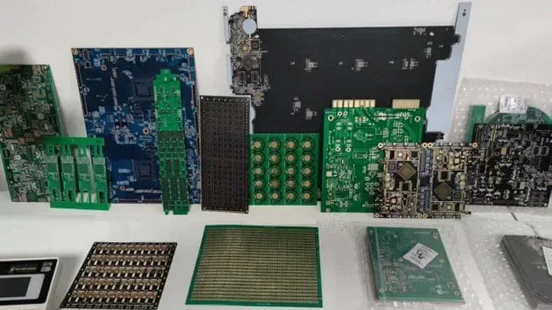
At PCBONLINE, we specialize in complex PCBs that require precision engineering and strict quality control, including:
- HDI PCBs – high-density interconnect boards for smartphones, wearables, and medical devices
- High-frequency PCBs – using Rogers or PTFE substrates for RF/microwave applications
- Flexible PCBs and rigid-flex PCBs – for compact, lightweight electronics
- Copper-core PCBs – with excellent heat dissipation for power electronics and LED lighting
- Ceramic PCBs – for high thermal conductivity and stable performance in aerospace and defense
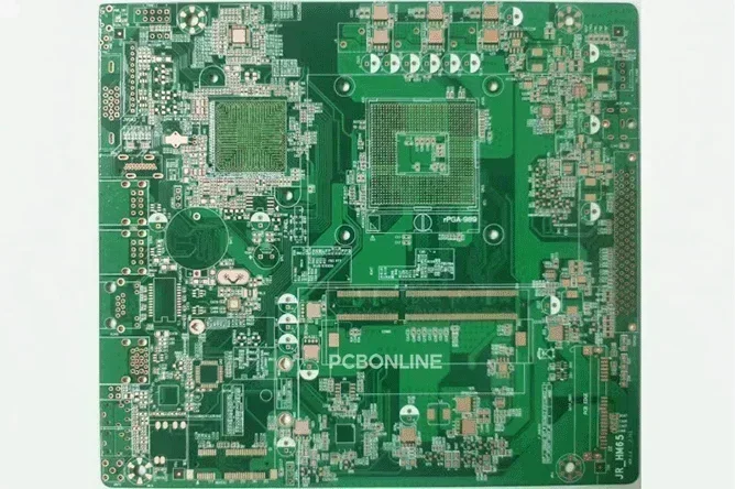
- Multilayer FR4 PCBs – up to 40+ layers with controlled impedance
The above advanced PCBs we provide go far beyond "cheap and simple". They are critical to the performance and reliability of critical industries.
Part 4. China PCB Fabrication Can Be Advanced – HDI PCB for Example
A great example of advanced China PCB fabrication is HDI PCB (High-Density Interconnect PCB).
HDI PCBs use microvias, buried vias, and blind vias to achieve high wiring density in small form factors. They enable thinner, lighter, and faster electronic devices.
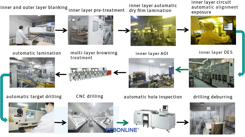
Fabricating HDI PCBs requires laser drilling, sequential lamination, resin plugging, and precise copper plating.
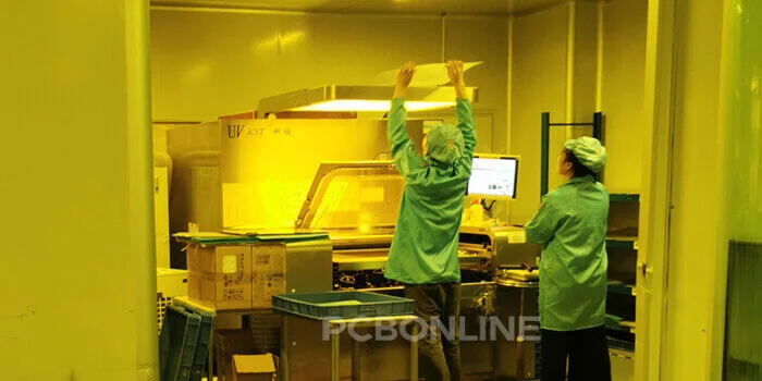
At PCBONLINE, our HDI PCB facilities and capabilities include:
Dedicated HDI production lines: automatic blanking and material prep; CCD LDI exposure for inner/outer layers; automatic DES (develop/etch/strip); browning lines for interlayer adhesion; lamination presses for sequential lamination; automatic target/CNC drilling; VCP (Vertical Continuous Plating) for uniform copper deposition; solder mask workshops with CCD alignment; ENIG/OSP/HASL surface-finish lines; V-cut and CNC profiling.
Factory throughput & stackup range: daily HDI capacity around 3,000 m² with 1+N+1 to 4+N+4 builds and up to 8 lamination/drill cycles when required. Minimum laser microvia = 0.075 mm; min. mechanical drill = 0.15 mm.
Inline inspection & test: online AOI, plating-thickness/X-ray checks, flying-probe and automatic E-test, four-terminal resistance test, dehumidification/leveling before pack-out.
Two in-house laboratories:
- Chemical lab for bath control, RoHS/REACH spot checks, and material verification.
- Physical lab for metallographic cross-sections, impedance measurement, withstand-voltage testing, and ionic contamination analysis
Meeting high demands: Multiple lamination cycles for complex designs, via-in-pad with copper filling for BGA/CSP packages, high layer counts with excellent reliability, and strict impedance control for high-speed signals
This shows that China PCB fabrication is not limited to prototypes or cheap PCBs. Our advanced PCB fabrication at PCBONLINE delivers one-stop solutions for mid and high-end applications.
Part 5. Partner with PCBONLINE for Advanced and Affordable PCBs
PCBONLINE is a trustworthy advanced PCB source factory manufacturer. We provide one-stop PCB and PCBA solutions from the initial ideas to the end products.
Founded in 2005, PBONLINE has two large advanced PCB manufacturing bases in Jiangsu and Jiangxi Provinces, and one PCB assembly factory in Shenzhen. It is a privately owned company that is ISO-verified.
PCBONLINE provide advanced PCB fabrication, PCBA assembly with component sourcing, and box-build assembly for system-level integration.
PCBONLINE is a source factory PCB manufacturer and offers affordable advanced PCBs.
No matter what quantity of boards you want, we prioritize quality, certified with ISO 9001:2015, ISO 14001:2015, IATF 16949:2016, RoHS, REACH, UL, IPC-A-600 Class 2/3, and IPC-A-610 Class 2/3.
PCBONLINE provides free engineering support for design optimization and DFM analysise.
Whether you need prototype development or mass production, we ensure reliability, precision, and cost-effectiveness.
Over teo decades, PCBONLINE has served many advanceed PCB and PCBA projects, such as electric vehicle charging stations, industrial transformer main boards, air conditioning central systems, military radar PCBs, medical PCBs, etc. And we have served many leader companies as below.
Our mission is to provide high-quality, advanced, and affordable PCBs for global clients. If you need to get a quote for PCB or PCBA, contact PCBONLINE by email at info@pcbonline.com.
Conclusion
China PCB fabrication is not just cheap and simple. With the right partner like PCBONLINE, it means advanced technology, complete solutions, and long-term reliability.
PCB Assembly from PCBONLINE.pdf
PCB fabrication at PCBONLINE.pdf


