
In the electronics manufacturing industry, SMT surface mount technology marks a major milestone in achieving fully automated, high-precision PCB (printed circuit board) assembly. Since PCBs serve as the foundation of almost all electronic systems and devices, a reliable SMT PNP (pick-and-place) assembly process is essential to ensure the quality and performance of electronic products. In this blog, PCBONLINE—a turnkey PCBA manufacturer—walks you through the SMT PNP process step by step, with detailed images.
In this article:
Part 1. What is SMT PNP? Part 2. Step-by-Step SMT PNP Process Part 3. Questions and Answers about the SMT PNP Process Complete the SMT PNP Process from the OEM PCB Manufacturer PCBONLINEWhat is SMT PNP?
SMT means surface-mounted technology, and PNP means pick-and-place.
In an SMT assembly process, components pick-and-place is the most important step. That's why a PCB SMT process is also known as the SMT PNP process.
The SMT PNP process is a key stage in PCBA manufacturing, where SMDs (surface-mounted devices) are accurately placed onto the pads of bare PCBs. These components are then permanently bonded through reflow soldering, forming reliable electrical and mechanical connections.
Compared with the PTH plated through-hole assembly process, the SMT PNP process is automatic and enables fine-pitch assembly. The advantages of the SMT PNP process are below.
Smaller electronics sizes: As electronic products become increasingly compact and intelligent, their PCBs must also be designed to fit smaller spaces. SMDs, used in the SMT PNP process, are much smaller than the bulky through-hole (PTH) components used in traditional assembly. SMDs support fine-pitch footprints such as 01005, 0201, 0402, and 0603—sizes that are impossible to achieve with PTH components.
More precision: The SMT PNP process is fully automated and highly precise. Both solder paste printing and component placement use advanced positioning technologies. Vision systems in the solder paste printer and pick-and-place machines detect fiducial marks on the PCB, enabling precise calibration and automatic compensation. These machines can also identify the center of each SMD pin and footprint, applying angle corrections to ensure accurate placement.
Higher production efficiency: The SMT process automates every step, from loading bare PCBs onto the line to final inspection with AOI (automated optical inspection). With no human intervention required during assembly, the process achieves high throughput and consistent quality. This makes it ideal for mass production and significantly lowers the cost per unit in PCBA manufacturing.
Proven reliability: The SMT PNP process has demonstrated reliable manufacturing quality over decades of use in the electronics industry. After reflow soldering, the solder joints form strong, lasting connections between the SMDs and the PCB. This process is trusted for critical applications in the medical, aerospace, military, and automotive sectors.
SMT assembly is versatile, and almost all components can be made into SMDs for surface mounting on the PCB. Except for high-power industrial controls like inverters that require a large area of through-hole assembly, all the other applications can be made from the SMT PNP process.
Step-by-Step SMT PNP Process
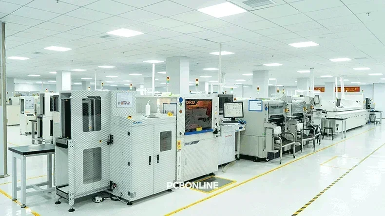
PCBONLINE, a professional OEM PCB manufacturer, operates its own PCB assembly factory capable of handling SMT and PTH assembly, component sourcing and management, box-build assembly, functional testing, and other value-added services. The factory is equipped with four dedicated SMT assembly lines to efficiently carry out the pick-and-place process.
SMT PNP process at PCBONLINE
Step 1. Loading bare PCBs
The process begins by loading bare PCBs onto the SMT line. Each PCB is placed in the slots of the loader, which is positioned at the start of the line. The loader feeds the PCBs into the production line for further processing.
Step 2. Solder paste printing
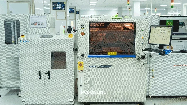
Once the bare PCB moves along the conveyor, it enters the solder paste printing machine. The machine's vision positioning system detects the PCB and aligns it precisely beneath the SMT stencil, ensuring the pads are perfectly matched with the corresponding stencil openings. At this point, the conveyor pauses.
A programmed scraper then moves across the stencil, pressing solder paste through the stencil openings onto the PCB pads. The speed, pressure, and angle of the scraper are all carefully controlled according to PCBONLINE's manufacturing specifications.
After printing, the conveyor resumes motion, moving the solder-pasted PCB out and feeding the next bare board into position.
Step 3. Solder paste inspection (SPI)
The PCB, now with solder paste applied, passes through a 3D SPI machine. Here, the board pauses as an infrared camera scans its surface. The system analyzes the captured image and compares it against a reference model.
If the solder paste's position, shape, and thickness meet quality standards, the SPI system displays a "PASS" result, and the PCB advances to the next stage: pick-and-place.
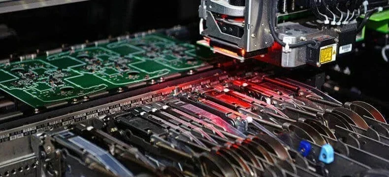
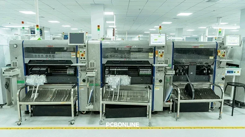
Step 4. Pick-and-place SMDs
PCBONLINE uses three advanced SMD pick-and-place machines in this stage: two high-speed Yamaha YSM20R high-speed machines and one functional YSM10 precision machine—among the most cutting-edge in the industry.
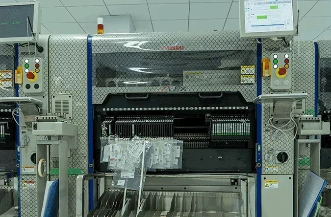
Each YSM20Rsupports up to 140 feeder slots and is responsible for placing small-footprint components such as resistors, capacitors, and inductors.
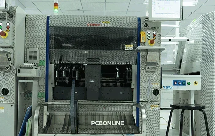
The YSM10 supports up to 96 feeder slots and handles components with larger footprints, such as ICs and connectors.
As the solder-pasted PCB moves through the PNP machines, each nozzle picks components from its designated feeder and accurately places them onto the PCB pads using a vision alignment system for maximum precision.
At this point, the board is fully populated with SMDs, completing the surface-mount stage of the process. It is now called a PCBA (printed circuit board assembly).
Step 5. AOI before reflow soldering
After component placement, the PCBA is transferred via conveyor to a 3D AOI machine for a pre-reflow quality check. The conveyor halts as infrared cameras scan the surface of the board.
The AOI system compares the scanned image with a reference model to detect any placement issues, such as missing or extra components, misalignment, polarity reversal, incorrect parts, or potential tombstoning.
The AOI before reflow helps identify and correct issues early, minimizing the risk of soldering defects and preventing costly errors later in production.
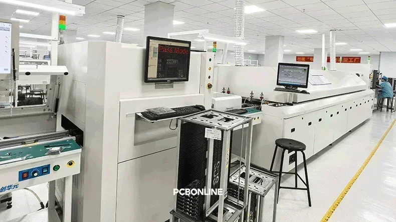
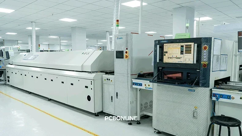
Step 6. Reflow soldering
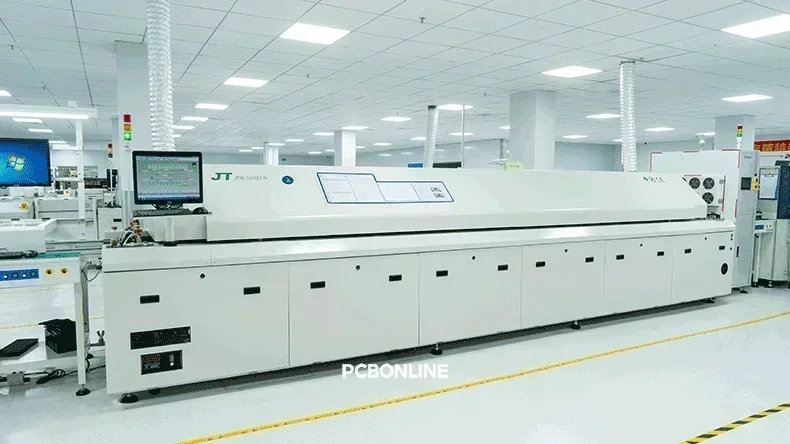
Once the PCBA passes AOI inspection, it proceeds into a lead-free reflow soldering oven. PCBONLINE's reflow ovens feature 10 temperature-controlled zones for preheating, soaking, reflow, and cooling.
At the peak temperature, the solder melts and undergoes a phase transition. The solder, PCB surface finish, and copper pad form a strong metallurgical bond.
This step solidifies the electrical and mechanical connection between the SMDs and the PCB.
Proper reflow soldering depends heavily on the speed and temperature profile. With extensive experience in SMT processes, PCBONLINE's engineers precisely program the reflow speed, guide speed, and temperature profile to suit the specific requirements of each PCBA project.
Step 7. AOI after reflow
After reflow, the PCBA moves to the final AOI station at the end of the SMT line. Here, the 3D AOI machine once again scans the board to ensure soldering quality.
The post-reflow AOI verifies that there are no defects such as solder bridging, tombstoning, insufficient or excess solder, solder balls, or irregular solder joint shapes. It also rechecks the accuracy of component placement, providing an additional layer of quality assurance before the next stage of production.
Questions and Answers about the SMT PNP Process
Q: What happens if any issue is found during the SPI and two AOI inspections? Will PCBONLINE repair them and test them again after repairing?
A: Yes. If any issues are detected during the SPI or AOI inspections, PCBONLINE immediately routes the affected boards to the In-Process Quality Control (IPQC) area for analysis and repairs. Besides repairing the issue, the IPQC technician reports the cause to the engineering team, helping in improving the SMT PNP process.
Once repaired, the boards are retested to ensure full functionality. These fixed boards are clearly separated from the smoothly processed ones throughout the rest of the production workflow to maintain quality traceability.
Q: Does PCBONLINE offer first-article inspection before mass SMT production?
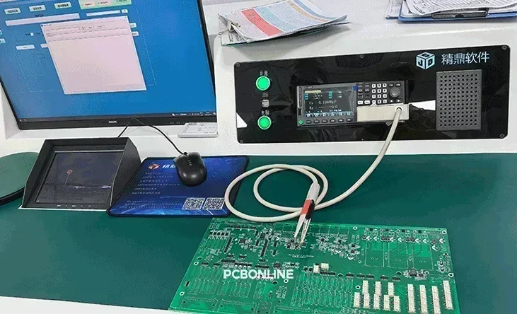
A: Yes, PCBONLINE performs a first-article inspection before beginning mass SMT production. After assembling the prototype PCBA, we conduct a detailed first-article inspection using test probes that clamp both sides of each SMD component. The component parameters are displayed on a screen to verify that they are within the specified tolerance range.
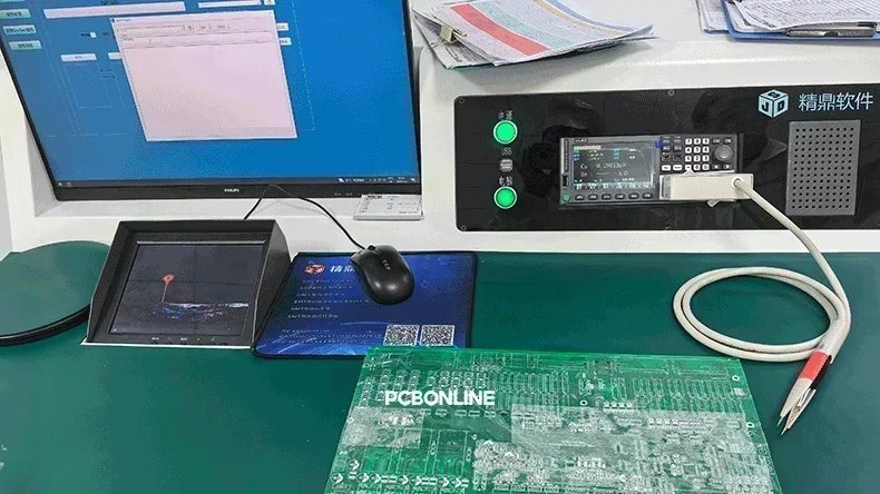
Besides, to further prevent potential losses, PCBONLINE performs another first-article inspection before assembling the prototype. We attach a layer of adhesive on the bare PCB, manually place the SMDs on it, and use the first-article inspection machine to clamp both sides of the SMDs. This ensures all component parameters are correct before actual assembly begins.
Q: It seems that the SMT PNP process at PCBONLINE doesn't have the X-ray inspection. How does PCBONLINE ensure the soldering quality of ICs in the BGA (ball-grid array) and QFN (quad flat no-lead) packages?
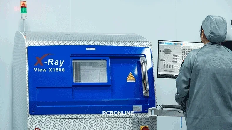
A: Nice question! PCBONLINE's PCB assembly factory is equipped with an X-ray inspection machine for ensuring the soldering quality of IC in no-lead and solder-balls packages, including BGA, QFN, DFN (dual flat no-lead), LGA (land grid array), and CSP (chip scale package).
The reason that the X-ray machine is not on the SMT line in this article is that the PCBA for SMT PNP assembly doesn't have ICs that require X-ray inspection. The SMT line is grouped by multiple machines, and the X-ray machine of PCBONLINE, which supports both in-line and off-line inspection, can insert the SMT line if required.
The X-ray inspection ensures that no-lead ICs and the solder balls/contacts between the PCB and the IC are soldered well.
Complete the SMT PNP Process from the OEM PCB Manufacturer, PCBONLINE
If your project requires both SMT and PTH assembly for electronics manufacturing, consider partnering with PCBONLINE, an OEM (Original Equipment Manufacturer) that delivers complete, turnkey solutions. PCBONLINE provides not only PCB assembly, but also PCB fabrication, component sourcing, mold and jig production, enclosure manufacturing, box-build assembly, value-added services, testing, and global shipping—delivering fully finished products you can sell on the market.
PCBONLINE is an OEM PCB source factory manufacturer founded in 1999. It has two large advanced PCB manufacturing bases independently fabricating all types of PCBs, one EMS (electronic manufacturing service) PCB assembly factory with two component warehouses, stable supply chains, and an R&D team. Besides, it keeps long-term cooperation with the top 3 mold/enclosure manufacturers in China to provide the molds, jigs, and enclosures for full box-build solutions.
Each SMT PNP line at PCBONLINE is equipped with three advanced pick-and-place machines, supporting up to 376 SMD placements per PCB, enabling us to handle all types of SMT assembly, including high-density and large-format boards.
Our SPI and dual AOI systems perform 3D surface scanning, offering thorough and accurate inspections for superior quality control throughout the process.
We conduct first-article inspections both before prototype assembly and before mass production to ensure the highest PCBA quality and prevent costly issues.
Our experienced R&D and engineering teams provide one-on-one support, solving technical and non-technical challenges while offering optimization suggestions to ensure your project runs smoothly from start to finish.
High-quality PCBA manufacturing certified with ISO 9001:2015, ISO 14001:2015, IATF 16949:2016, RoHS, REACH, UL, and IPC-A-610 Class 2/3.
When your project enters the bulky production stage, PCBONLINE refunds the fees of prototyping, including its value-added services.
No matter what quantity of boards you order, PCBONLINE prioritizes quality. To get a quote from the SMT PCBA manufacturer PCBONLINE, contact info@pcbonline.com.
Conclusion
This article demonstrates the PCB pick-and-place process on an advanced SMT line at PCBONLINE. To ensure the success of your PCB/PCBA projects, work with the turnkey advanced PCB manufacturer PCBONLINE.
PCB assembly at PCBONLINE.pdf


