

The humble printed circuit board (PCB) is the foundation of electronic devices, from AI servers to industrial control systems. PCB drawing file, the digital blueprint, tells machines where to etch copper, where to drill holes, and where to place components.
The global PCB design software market is currently experiencing a massive surge. Valued at approximately USD 5.43 billion in 2025, it is projected to more than double, reaching over USD 14 billion by 2033. This 12.8% compound annual growth rate highlights a world that is becoming more connected and more automated every day.
In this guide, we will dive deep into the world of PCB drawing files, the software used to create them, and the professional workflows that ensure your designs transition perfectly from the screen to the factory floor.
Why PCB Design is Booming
The growth in the PCB software market is driven by the increasing complexity of electronics. North America currently leads this charge, holding over 36.4% of the global market share. This dominance is fueled by heavy investments in aerospace, defense, AI servers, and high-end consumer electronics.
Interestingly, the software segment itself accounts for 84% of the industry's revenue. This tells us that engineers are looking for sophisticated Electronic Design Automation environments that can handle complex simulations, supply-chain data, and collaborative features.
Whether you are a hobbyist using open-source tools or a professional engineer at a Tier-1 manufacturer, the quality of your drawing files determines the success of your product.
What is a PCB Drawing File?
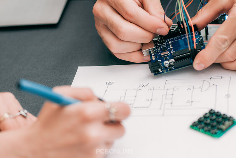
A PCB drawing is much more than a simple picture. It is a data-rich set of instructions. When we talk about "drawing files" in a professional context, we are usually referring to a collection of files generated by EDA software.
Core inputs for a PCB design
Before a single trace is drawn, four critical pieces of information must be established:
- The schematic: The logical map of the circuit, showing how components connect.
- Mechanical constraints: The physical size of the enclosure, the location of mounting holes, and the height limits for components.
- Bill of materials (BOM): A comprehensive list of every component required.
- Routing guidelines: Rules regarding high-speed signals, power requirements, and sensitive trace paths.
The final output is a package of files in Gerber or ODB++ format. It describes every layer of the PCB, from the internal copper planes to the green solder mask and the white silkscreen lettering.
Professional PCB Design Workflows
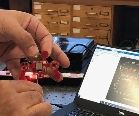
Creating a high-quality PCB drawing requires a disciplined workflow. It connects the dots and ensures the PCB can actually be built, tested, and used in the real world.
Step 1: Schematic capture and component assignment
The process begins by drawing the electrical circuit. Here, every symbol is linked to a specific physical footprint. If you choose a resistor, the software must know exactly how large that resistor is so it can reserve the right amount of space on the PCB.
Step 2: PCB outline and stackup
Next, you define the PCB's physical boundaries. You also decide the stackup—how many layers of copper and insulation the PCB will have. This is crucial for managing heat and electrical interference.
Step 3: Placement and routing
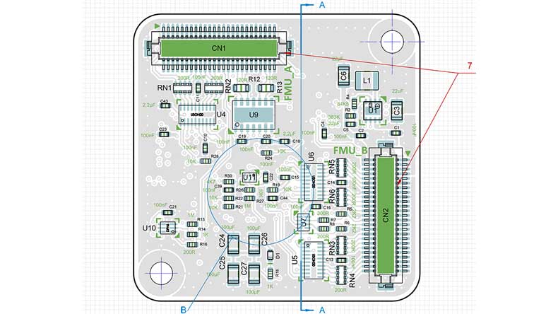
This is the "drawing" phase. Components are placed for optimal performance, and copper traces are routed to connect them. Engineers must follow specific rules here. For example, in software like KiCad, differential pairs (used for high-speed data) must be labeled with specific suffixes like '+' and '-' or 'P' and 'N' so the software knows to keep them perfectly parallel.
Step 4: The DFX review
This is where professional services like PCBONLINE provide immense value. Before the files are sent to the machines, they undergo a series of "Design for Excellence" (DFX) checks:

- DFM (Design for Manufacturing): Can the factory physically etch and drill this PCB?
- DFA (Design for Assembly): Can the components be soldered without interference?
- DFT (Design for Test): Are there points where we can test the PCB after it's built?
By integrating these checks early, you avoid costly mistakes and "re-spins" (having to redesign the PCB from scratch).
Industry Standards: IPC-2152 and IPC-2221
To ensure reliability, PCB drawings must adhere to international standards.
- IPC-2221: This is the gold standard of PCB design. It provides the generic standards for spacing, land patterns, and general manufacturability.
- IPC-2152: This standard is used for calculating conductor widths. If you are running high current through a board, you need to know exactly how wide the copper trace must be to prevent it from overheating. Tools like the Saturn PCB Toolkit use these standards to help engineers get the math right every time.
PCB Design Software Comparison
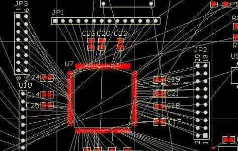
The market offers a wide range of tools, from free community projects to high-end enterprise suites. Your choice depends on your budget and the complexity of your project.
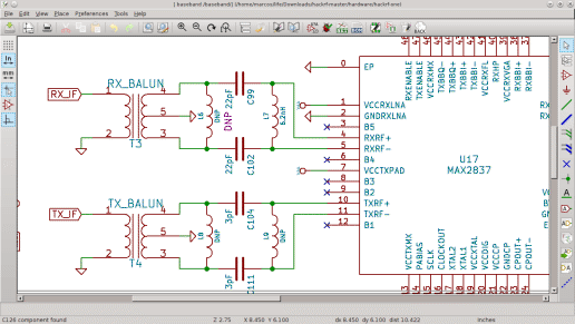
KiCad: The open-source powerhouse
- Cost: Free.
- Best for: Teams needing zero licensing costs and full control over their data.
- Key feature: It runs on Windows, macOS, and Linux. It has a robust community and is powerful enough for complex multi-layer PCBs.
EasyEDA: The browser-based beginner
- Cost: Free tier; $19.90/month for Premium.
- Best For: Fast prototyping and hobbyists.
- Key feature: It is highly integrated with parts suppliers, making it easy to order components directly from the design interface.
Autodesk Fusion: The all-in-one solution
- Cost: Approximately $680/year.
- Best for: Products wherethe PCB must fit perfectly into a complex mechanical housing.
- Key feature: It combines PCB design with 3D mechanical CAD, allowing you to see your board inside its box before you build it.
Altium Designer: The industry standard
- Cost: Starting at $355/month.
- Best for: High-end professional design and corporate environments.
- Key feature: Advanced cloud collaboration and powerful routing tools. It is widely used in professional design houses globally.
Cadence OrCAD X: The supply-chain intelligent
- Cost: Private pricing.
- Best for: Enterprise-level manufacturing.
- Key feature: It features "Live BOM" intelligence, providing real-time data on over 1.6 billion parts. This ensures you don't design a board using a part that is out of stock or discontinued.
From Drawing to Reality: Working with PCBONLINE
Even the most beautiful drawing file is useless if it cannot be manufactured correctly. This is why many engineers partner with turnkey providers like PCBONLINE.

Founded in 2005, PBONLINE has two large advanced PCB manufacturing bases and one PCB assembly factory.
PCBONLINE acts as the bridge between your digital drawing and the physical product. They work with files from almost all major EDA environments, including Allegro, Altium, Protel, Autodesk Eagle, and KiCad.
When you submit your drawing files to a high-end fabricator, we perform a rigorous layout review.
At PCBONLINE, we check your Gerber files and BOM against current industry standards like ISO9001:2015 and IATF 16949 (the automotive standard).
For industries like medical or aerospace, we ensure compliance with REACH, RoHS, and UL standards.
We can even achieve assembly lead times as short as 8 hours for urgent projects. This speed is only possible because of the precision of the initial drawing files and the sophisticated software used to verify them.
At PCBONLINE, we can help our clients reduce costs while achieving the highest levels of performance and reliability. If you feel interested in PCB fabrication and assembly from PCBONLINE, send your inquiry by email to info@pcbonline.com.
Best Practices for PCB Drawing
If you want your PCB design to be successful, keep these three tips in mind:
Optimize your track widths
Always use design rules to set minimum, optimal, and maximum track widths. For instance, in KiCad, you might set a minimum of 0.5 mm for a power trace. If you accidentally draw it thinner, the Design Rule Check (DRC) will flag it as an error. This prevents "burnt" traces in your final product.
Embrace supply-chain visibility
The "chip shortage" taught the industry a hard lesson. Today, the best software (like OrCAD X) shows you part availability while you are drawing. Don't wait until the PCB is finished to find out that your main microcontroller has a 52-week lead time.
Think about the box
Never design a PCB in a vacuum. Use 3D views to ensure that tall components (like capacitors) won't hit the lid of your enclosure. Integrated tools like Autodesk Fusion make this seamless.
The Future: AI and Automation in PCB Design
As the market grows toward that $14 billion valuation in 2033, we can expect to see even more automation. Artificial Intelligence is beginning to assist with auto-routing, helping engineers find the most efficient paths for thousands of traces in a fraction of the time it would take a human.
However, the core of the industry remains the same: a high-quality, standardized drawing file is the only way to ensure reliability. Whether you are using the free KiCad or the premium Altium, your goal is to create a digital twin of your physical product that is so accurate that a machine halfway across the world can build it without a single phone call for clarification.
Conclusion
The world of PCB drawing files is evolving from simple 2D layouts into complex, data-rich ecosystems. With the market set to explode over the next decade, staying informed about the latest software, standards like IPC-2221, and manufacturing workflows is essential for any electronics professional. By choosing the right software and partnering with a reliable manufacturer like PCBONLINE, you can turn your innovative ideas into high-quality, reliable hardware.
PCB assembly at PCBONLINE.pdf


