
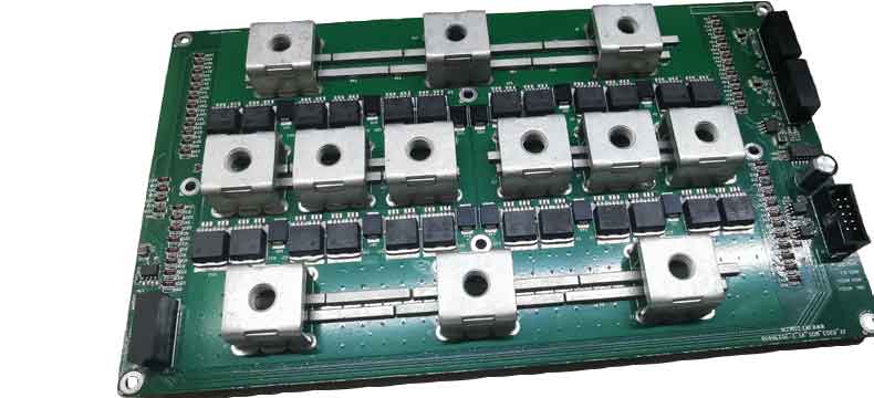
In the manufacturing of almost all electronic products and hardware systems, a printed circuit board (PCB) is the foundation for a fully functional electronic product. The transformation from a bare PCB to a populated printed circuit board is a critical stage in electronics manufacturing. Electronic components are assembled, soldered, tested, and prepared for integration into end products.
In this article:
Part 1. Is a Populated Printed Circuit Board a PCBA? Part 2. Printed Circuit Board Assembly Process Part 3. Advice on PCB Design and BOM
Is a Populated Printed Circuit Board a PCBA?
Yes, a populated PCB is exactly a PCBA.
Whether you are a hardware startup, an OEM, or an engineer managing outsourced manufacturing, it's important to understand what a populated PCB is, the PCB assembly (population) process, PCB design, and making Bill of Materials (BOM) decisions.
The terms populated printed circuit board and PCBA (Printed Circuit Board Assembly) are used interchangeably.
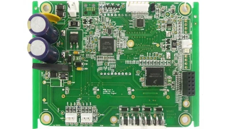
A printed circuit board (PCB) by itself is a bare electronic circuit board made of insulating material (FR4, aluminum, polyimide, copper, PTFE, or ceramic) with copper traces etched onto it. At this stage, it contains no electronic components and cannot perform any electrical function.

Once electronic components are mounted and soldered onto the PCB, the circuit board becomes a populated printed circuit board. The populated PCB is commonly referred to as a PCBA.
Here are the electronics manufacturing terms related:
- PCB = bare circuit board with copper traces, pads, and vias
- Populated PCB = PCB with components installed
- PCBA = industry-standard term for a populated PCB
Therefore, a populated printed circuit board is a PCBA.
However, context matters. The phrase populated printed circuit board is often used in descriptive or marketing language to emphasize the physical state of the circuit board, while PCBA is more commonly used in technical documentation, contracts, and manufacturing workflows.
Printed Circuit Board Assembly Process
The PCB assembly process is the bridge between electronic design and real-world products. It converts a bare PCB and loose components into a functional electronic module ready for testing, enclosure assembly, or system integration.
While details may vary depending on product complexity, volume, and technology, the standard PCBA process generally follows the steps below.
1. PCB Fabrication (Pre-Assembly Step)
Before PCB assembly can begin, we fabricated the PCB according to the design files. (We are a turnkey PCBA manufacturer with two advanced PCB manufacturing bases and one PCB assembly factory.) This includes:
- Copper layer imaging and etching
- Drilling and plating vias
- Solder mask application
- Silkscreen printing
- Surface finish (HASL, ENIG, OSP, etc.)

Although PCB fabrication is not assembly, its quality directly affects assembly yield, solderability, and long-term reliability. So we suggest that you can also handle PCB manufacturing and component sourcing for us, as we can ensure the PCB and component quality.
If your PCBs or components have been prepared by other suppliers, we will check your PCBs and components carefully, including X-ray and IC counterfeit testing. If these PCB and components needs baking, we will bake them. The testing and baking may generate a small amount of additional fees.
2. Solder Paste Printing
PCB assembly begins with solder paste application. A stainless steel stencil, which is already set in the solder paste printing machine, is aligned over the PCB, and solder paste is deposited onto the component pads of the PCB.
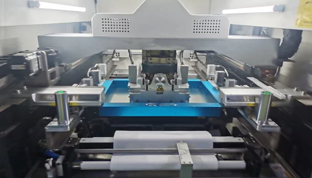
Our engineers have rich experience with the PCBA manufacturing process designs, and we take care of these factors in the soldering paste printing stage:
- Stencil thickness and aperture design
- Solder paste type (standard framed/frameless or step-up/down)
- SMT stencil aperture design
- Environmental control (temperature and humidity)
Accurate solder paste printing is critical, as insufficient or excessive paste can cause defects such as tombstoning, solder bridges, or weak joints.
Our EMS PCB assembly ensures that product design and manufacturing are aligned from the very beginning.
3. Component Placement (SMT Assembly)
Most populated printed circuit boards rely heavily on Surface Mount Technology (SMT).
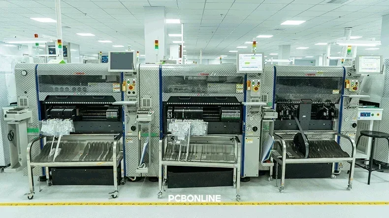
At PCBONLINE, every SMT line uses three automated pick-and-place machines — two YAMAHA YSM20R and one YAMAHA YSM10. Supporting 376 SMD devices for a side of each PCB:
- Components are picked from reels, trays, or tubes
- Parts are placed onto solder paste deposits with high precision
- Placement data is derived from centroid (XY) files
SMT enables high component density, reduced PCB size, and excellent electrical performance. For high-volume PCBA production, placement accuracy and speed are optimized to achieve consistency and efficiency.
4. Reflow Soldering
Once components are placed, the populated circuit board passes through a reflow oven. However, PCBONLINE adds a pre-reflow automated optical inspection (AOI) to check the component placement effect before reflow soldering.
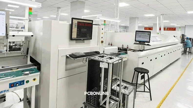
During reflow, controlled temperature profiles melt the solder paste and form permanent electrical and mechanical connections.
A reflow profile includes:
- Preheat
- Soak
- Reflow peak temperature
- Controlled cooling
Proper thermal profiling is essential to prevent component damage, cold solder joints, or voiding, especially for fine-pitch ICs and BGAs.
5. Through-Hole Assembly (If Required)
Some designs still require through-hole components, such as:
- Power connectors
- Transformers
- Large capacitors
- Mechanical reinforcement parts
Through-hole assembly is done half manually and using wave soldering or selective soldering processes. Many populated PCBs use a mixed-technology approach, combining SMT and through-hole components.
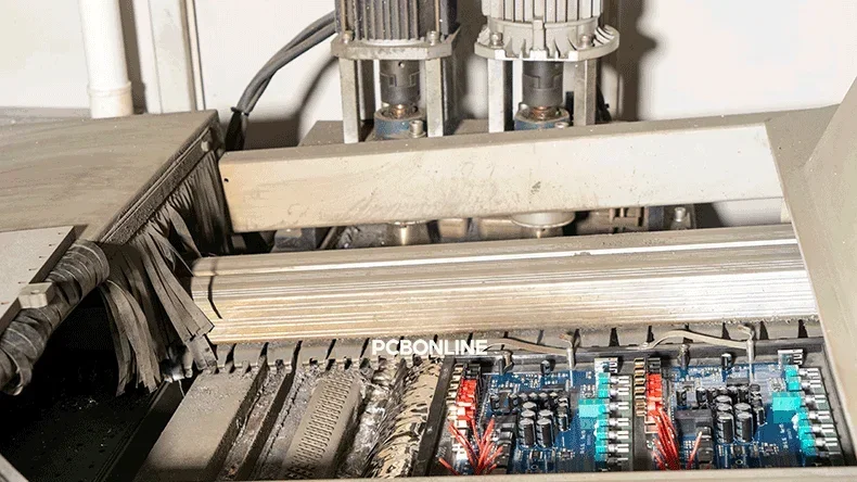
At PCBONLINE, we have four through-hole assembly lines with four wave soldering ovens and one selective soldering line.
6. Inspection and Quality Control
Inspection ensures that the populated PCB meets electrical and mechanical standards. On our PCB assembly lines, the inspection methods include:
- Dual-AOI (Automated Optical Inspection) for solder joints and placement
- X-ray inspection for hidden joints (e.g., BGA, QFN)
- Manual visual inspection for special or low-volume PCBAs
Inspection reduces the risk of latent failures and improves overall product reliability.
7. Electrical Testing
Testing verifies that the assembled PCB functions as intended. Depending on the product, the electrical tests may include:
- In-circuit testing (ICT)
- Flying probe testing
- Functional testing
- Power-on testing
Well-designed test points and clear test procedures significantly reduce debugging time and production scrap rates.
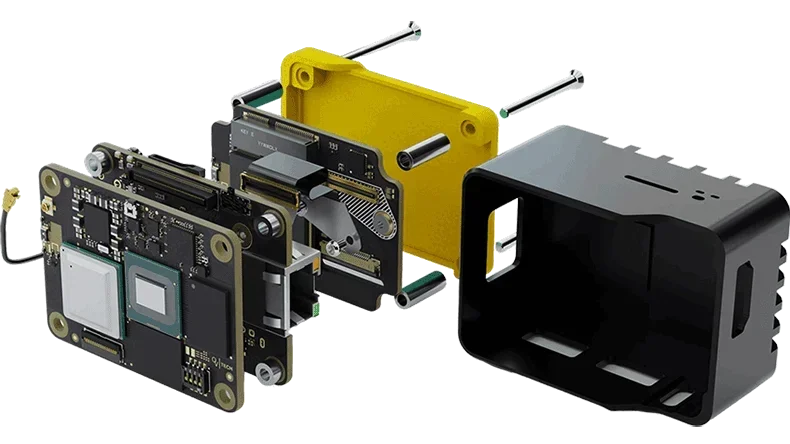
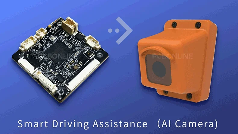
8. Final Assembly and Integration
Once PCB assembly and testing are complete, the populated printed circuit board may be:
- Installed into an enclosure
- Connected with cables or harnesses
- Integrated into a larger system or product
At this stage, the PCBA transitions from an electronic subassembly into a finished or semi-finished product.
When the semi-finished device passes the FAE (Field Application Engineering) tests and is labeled and packaged, it becomes a final product.
Advice on PCB Design and BOM
Successful PCB assembly does not begin on the factory floor, but starts at the design and BOM stage. Poor design choices or incomplete documentation can dramatically increase costs, delays, and defect rates.
Below are practical recommendations to improve manufacturability and scalability.
PCB Design for Assembly (DFA)
Designing with assembly in mind is one of the most effective ways to reduce risk.
PCB design considerations include:
- Component spacing: Ensure adequate clearance for placement and soldering
- Standard package sizes: Avoid uncommon footprints unless necessary
- Consistent orientation: Align polarized components uniformly
- Solder mask openings: Optimize for reliable solder joints
- Panelization strategy: Design boards that can be efficiently panelized
Following DFA guidelines improves yield, reduces rework, and lowers production costs, especially in volume manufacturing.
Thermal and Power Considerations
Populated printed circuit boards must handle real operating conditions.
Designers should consider:
- Copper thickness for current-carrying traces
- Thermal vias for heat dissipation
- Proper placement of heat-generating components
- Ground planes for noise and thermal stability
Ignoring thermal design often leads to premature field failures, even if initial testing passes.
Clear and Complete Manufacturing Files
PCBA manufacturers like PCBONLINE rely on accurate documentation. Essential files include:
- Gerber or ODB++ files
- Pick-and-place (centroid) files
- Assembly drawings
- Test requirements
- Programming instructions (if applicable)
Incomplete or inconsistent files slow down quoting and increase the risk of errors.
BOM Optimization and Management
The Bill of Materials (BOM) is as important as the PCB layout.
Recommended BOM practices include:
- Use readily available components with multiple suppliers
- Avoid parts near end-of-life
- Standardize values where possible
- Specify manufacturer part numbers (MPNs) clearly
- Include approved alternates
A well-structured BOM reduces procurement risk, stabilizes pricing, and prevents production delays caused by component shortages.
Design for Scalability
Many products start with low-volume prototypes and later scale to mass production. Planning for this transition early is important.
To support scalability:
- Avoid hand-solder-only components
- Minimize manual assembly steps
- Use automated test strategies
- Select components suitable for reflow profiles
Designing for scale ensures your populated printed circuit boards can move smoothly from prototype to production without costly redesigns.
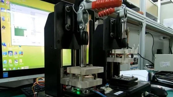
Partner with PCBONLINE for OEM PCB Assembly
PCBONLINE is a turnkey PCBA manufacturer providing OEM (original equipment manufacturer) PCB assembly. We provide all the electronics manufacturing and materials used for our PCB box-build assembly services, including the PCB enclosures.
Our OEM PCBA manufacturing services offer:
- Complete procurement: We source and customize enclosures, cables, and accessories from reliable suppliers.
- Engineering support: We check enclosure and accessory designs for compatibility with your PCBA and can suggest design changes.
- Free DFM/DFT: We provide free Design for Manufacturability (DFM) and Design for Testability (DFT) checks to ensure that designs are optimized for a smooth production process.
- Special capabilities: IPX8 waterproof enclosures and encapsulation for rugged outdoor devices.
- Quality assurance: IPC-A-610 Class 3, automotive-grade or industrial-grade inspection standards.
- Turnkey delivery: From PCB fabrication to final product packaging and shipping.
- Testing and value-added services: Offering a range of quality assurance services, including X-ray inspection for hidden-joint PCBAs, first-article inspection, PCBA functional testing (FCT), IC programming, burn-in test, PCBA coating, enclosures, and box-build assembly.
Founded in 2005, our two advanced PCB manufacturing bases are in Jiangsu and Jiangxi Provinces, and our turnkey PCB assembly factory is in Shenzhen. Besides, we have an R&D team and a global supply network. We also maintain strategic cooperation with the top 3 fixture and enclosure factories in China to manufacture the custom PCBA fixtures and device enclosures.
PCBONLINE manufactures, assembles, and tests PCBs and PCBAs to box builds as a source factory manufacturer under one roof, from prototypes to bulky production, saving costs and time for you.
We keep strategic cooperation with the top 3 enclosure manufacturers in China to manufacture custom device enclosures.
We can design the PCB enclosure to match your PCB. Besides, we can help create user manuals, installation guides, and compliance labels.
Our high-quality PCBA contract manufacturing is certified with ISO 9001:2015, ISO 14001:2015, IATF 16949:2016, RoHS, REACH, UL, and IPC-A-610 Class 2/3.
Our one-on-one free and professional DFM helps you debug and improve design, to ensure the manufacturability, cost-effectiveness, and final device success.
Whether you need OEM PCB assembly to build consumer IoT devices, creative electronic products, automotive/medical-grade systems, etc, with 20 years of PCBA manufacturing and box build experience, we ensure that both electronics performance and final product presentation meet the highest standards. To get a quote for your EMS PCB assembly project, email us at info@pcbonline.com.
Conclusion
A populated printed circuit board represents far more than a PCB with components attached—it is the functional core of almost every modern electronic product. By integrating design, BOM, PCBA manufacturing, testing, and enclosure development into a single workflow, our OEM PCB assembly service reduces complexity, lowers costs, and improves product quality. Contact us to build OEM PCBA or box-builds to deliver your products to success. (We do not make hobbdyiest PCBs.)


