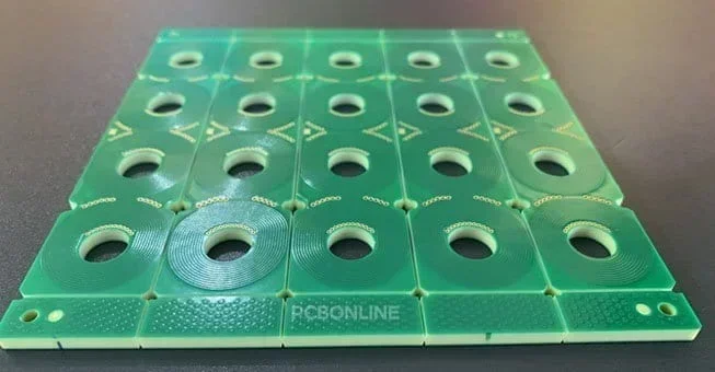
A PCB, or printed circuit board, is a laminated board made of copper traces, insulated materials, and substrate materials. It is manufactured from Gerber, the PCB design file containing the PCB layers that tell the PCB manufacturers what the PCB requirements are in graphics.
Do you understand the different PCB layers in the Gerber? This article will introduce the PCB layers in the Gerber individually for you.
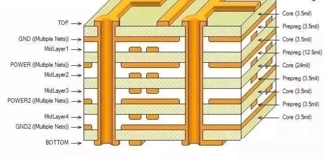
Different PCB Layers
In a Gerber, each PCB layer corresponds to a file in the Gerber. The PCB layers are below.
Mechanical layer: It defines the PCB panelization boards' physical outline specs.
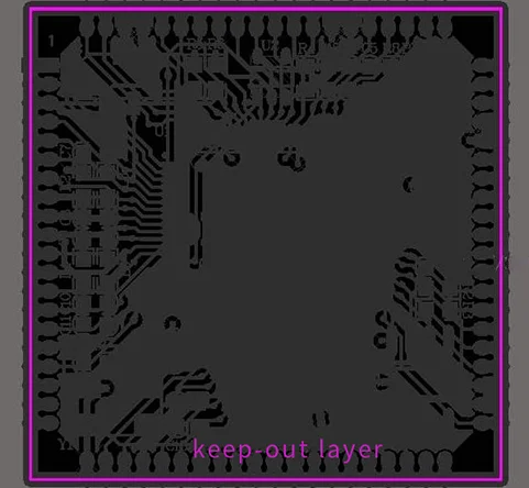
Keep-out layer: It defines the border of the electronics area on the PCB. Wiring and electronic functions are restricted in this area.
Signal layers: They define the wires on the circuit board. The PCB design program Protel 99 SE has 32 signal layers, including the top, Bottom, and 30 MidLayers.
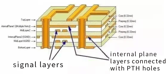
Internal plane/ground layer: It defines the wiring of power and ground lines in multilayer PCBs. Also, use Protel 99 SE as an example, it provides 16 internal power/ground layers for PCB design.
Top overlay layer: It is the silkscreen on the upper side of the PCB. It defines the component codes, symbols, and some frames on the PCB's top side.
Bottom overlay layer: It is the silkscreen on the bottom side of the PCB. It defines the component codes, symbols, and some frames on the PCB's bottom side.
Top paste layer: It defines the PCB pads on the upper side of the board. It is the solder mask openings used for SMT stencil printing the solder paste and glue dosing for some surface-mount devices (SMDs) on the PCB's top side.
Bottom paste layer: It defines the PCB pads on the bottom side of the board. It is the solder mask openings used for SMT stencil printing the solder paste and glue dosing for some surface-mount devices (SMDs) on the PCB's bottom side.
Note: The top and bottom paste layers together are called the paste mask layers.
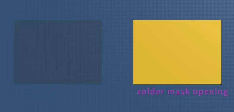
Top and bottom solder layers: They define the solder masks on the upper and bottom sides of the PCB. PCB inks are applied to protect the PCB copper from oxidation and mechanical damage. (By default, in the top/bottom solder paste layer, if you don't select any area, it means the entire side is printed with solder mask oil. If you select some areas, it means they are the solder mask openings for solder paste printing.) The top and bottom solder layers together are called the solder mask layers.
Drill guide: It is a table listing the PCB diameters and corresponding symbols.
Drill drawing layer: It defines the positions and drill size of the PCB holes.

Multilayer: It defines the same position of a PCB pad in all the PCB layers (AKA the hole).
One-Stop Advanced PCB Manufacturer Custom Meeting Your Demands
If you need PCB fabrication and assembly under one roof, including the R&D and end device assembly, you can work with PCBONLINE. PCBONLINE is an advanced PCB manufacturer that manufactures and assembles any type of PCB no matter what layer account of the PCB is.
Founded in 1999, PCBONLINE has two large advanced PCB manufacturing bases, one PCB assembly factory, stable supply chains, and an R&D team for one-stop PCBA manufacturing.
PCBONLINE has strong PCB manufacturing capabilities, including FR4 PCB layers from 1 to 64, high-density PCB, high-frequency PCBs, flexible PCB, rigid-flex PCB, aluminum PCB, copper-based PCB, and ceramic PCB.
PCBONLINE offers free design for manufacturing (DFM) for your PCB and PCBA project, including checking Gerber, bill of materials (BoM), testing files, and solving all technical and unexpected issues during prototyping to ensure a smooth and successful massive production.
PCBONLINE can do the R&D for your PCBA project or take part in your project's development from the early stage for the optimum PCB design and prevent tricky problems in the field application engineering (FAE) stage.
One-stop PCB services meet your custom needs, including prototyping/sampling, PCB manufacturing, component sourcing, PCB assembly, PCBA value-added, enclosure, and box-build assembly.
High-quality advanced PCB manufacturing certified with ISO 9001:2015, ISO 14001:2015, IATF 16949:2016, RoHS, REACH, UL, and IPC-A-600 Class 2/3.
No matter what quantity of PCBs you want, PCBONLINE offers one-on-one engineering support for your project all the way. To get a quote for your PCB project, contact info@pcbonline.com.
Conclusion
The PCB design file Gerber contains many PCB layers. This blog introduces the different layers of meaning in the Gerber one by one. If you want to learn more about advanced PCB or have your PCB project into production, chat with the one-stop PCB manufacturer PCBONLINE from the online chat window.
PCB assembly at PCBONLINE.pdf


