PCB (printed circuit board) design and assembly are crucial processes in electronic manufacturing. Any electronic device's sensory system is a PCB, which connects and supports various circuits and components. PCB design involves positioning and aligning various electronic components on the board, ensuring everything works harmoniously to bring an electronic device to life. The PCBA (printed circuit board assembly) process involves the placement of electronic components, followed by their precise soldering and the ultimate creation of a fully functional electronic device.
During PCB design, careful planning is required to optimize performance, minimize signal interference, and make efficient use of available space. During PCB assembly, the PCB is loaded with components such as integrated circuits, resistors, capacitors, and connectors. Accuracy is essential while building something to guarantee dependability and proper performance.
What to Take Care of in PCB Design
The PCB design process involves sketching up a layout showing where electrical components are placed and connected. Schematic capture, component placement, routing traces, and taking power distribution, signal integrity, and manufacturability into consideration are common processes.
PCB Design Process
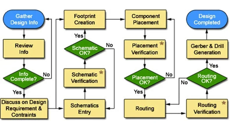
The PCB design process is a systematic approach to designing the layout and arrangement of electronic components on a circuit board. This crucial stage bridges the gap between the design of an electrical device and its actual construction. The following is a summary of the PCB design process.
Project Definition
In the initial phase of PCB design, requirements and specifications become critical because the project objectives, performance measures, and regulations are all spelled. To do so, one has to define key performance indicators, comply with industry standards, and take into consideration the demands of components, time, and money.
A comprehensive risk assessment, cooperative strategies, and scalability further provide a solid grounding for the entire design process. This approach guarantees that the latter phases are in line with project goals hence facilitating effective and successful implementation of PCB designs.
the temperate control system used for the greenhouse effect
Perform Criteria
Determining performance criteria, or establishing and identifying the critical metrics that govern the effectiveness and functioning, is an essential phase in the PCB design process. Such criteria include processing speed, power consumption, and environmental impact among other issues that relate to reliability. These predetermined criteria must be surpassed by or at least met by PCBs through careful examination thus providing a clear roadmap for maximizing overall system performances of electronic systems. Performance requirements therefore need to be specified at the early stages of design to guarantee that a PCB is delivered in conformity to its intended application and user expectations.
Regulatory Compliance
An important part of PCB design is regulatory compliance. A product must meet industry and legal guidelines in terms of use or the making of electronic devices. As such, it is necessary to go through all applicable regulations, safety precautions, and EMC (electromagnetic compatibility) standards. These parameters ensure the safety of users, the reliability of products, and the ease of interacting with the regulatory framework.
It is up to the designer to guarantee that the PCB adheres to these rules. All necessary modifications are made to ensure that the design satisfies the specifications. Thorough documentation and testing are essential for verifying adherence. Proactive approaches towards regulations within PCB designs not only satisfy legal requirements but also set a basis for reliable and economically successful electronic products.
Budget and Timeline
Along with determining realistic financial limits and establishing a deadline, managing money and timeframe effectively is one of the crucial elements in PCB design. Regarding the cost of purchasing, fabrication, and testing of components, designers have to be economical in their use of resources. Meanwhile, there will be a clear timetable with critical milestones that will enable tracking progress as well as meeting project completion dates.
To reconcile the requirement to produce a high-quality PCB with financial constraints, the budget and schedule must be regularly reviewed and modified during the design cycle.
Component Requirements
A designer should ensure that the electronic components that make up the circuit are properly for meeting component requirements in PCB design. Designers have to indicate the required types and qualities of components, taking into account such factors as cost, compatibility, and usefulness.
A critical analysis of part availability and viable substitutes results in a firm design that aligns with the technical requirements and financial constraints.
Scalability and Future Considerations
Further considerations in the future require that designers examine how robust their work will be when it comes to upgrades or modifications. This includes looking at market trends, technological advances, and possible changes in project parameters going forward. With its scalability-conscious design, the PCB can resist future expansions or updates without needing to be completely redesigned.
Using a flexible design approach and accounting for emerging technology extends the life and usefulness of the electronic system. This establishes the foundation for further creativity and adaptability as the project grows. This perspective ensures that the PCB will remain viable and functional for an extended time.
Collaboration and Documentation
Collaboration and documentation ensure communication and thorough records throughout the entire design journey. Within the design team having roles and responsibilities promotes teamwork. This documentation proves invaluable when it comes to design iterations, troubleshooting, and sharing knowledge among team members. Efficient collaboration and meticulous documentation not only strengthen team cohesion but also preserve institutional knowledge and facilitate smooth transitions between different phases of PCB design.
Risk Assessment
Conducting a risk assessment is a step in the PCB design process. This involves identifying and evaluating obstacles or uncertainties that could impact the project. Designers proactively consider factors such as component accessibility, production complexities, and external market influences. The goal is to anticipate risks by developing alternative strategies to address challenges.
By systematically addressing uncertainties early in the design phase, the risk assessment lowers the likelihood of issues during manufacturing and testing. By assuming measured risk, the PCB design process remains adaptable and responsive to unforeseen challenges, thus increasing the project's overall success.
To sum up, a comprehensive risk assessment makes it easier to recognize and address potential roadblocks, which in turn creates a resilient design that can effectively handle uncertainty during the manufacturing and testing stages.
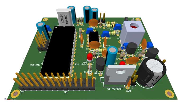
Example of PCB design Practical -- Full Wave Rectifier
Creating a PCB for a full-wave rectifier is a significant and fascinating undertaking in the field of electronics. The full-wave rectifier is a crucial circuit for changing alternating current (AC) to direct current (DC) and powering several electronic devices.
In this practical study of PCB design, we explore the challenges of designing a compact and efficient architecture for the full-wave rectifier circuit. This project integrates theory and real-world experience, from understanding capacitor and diode specs to positioning parts to reduce signal interference.
Along the process, we hope this example can enhance your ability to design PCBs and deepen your comprehension of the vital function that these circuits play in the field of electronics.
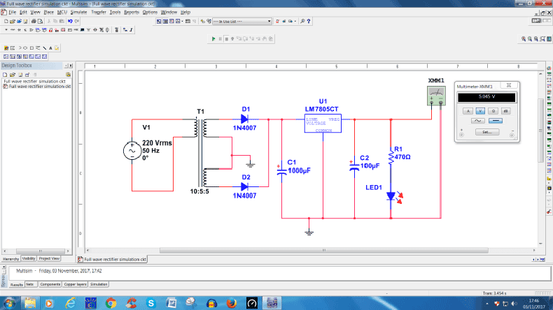
Circuit of Full Wave Rectifier Before Simulation
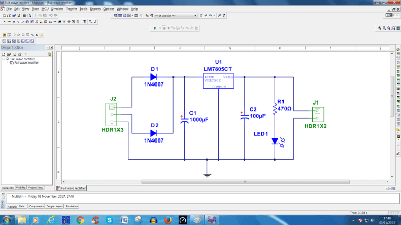
MULTISIM to ULTIBOARD single side PCB Design
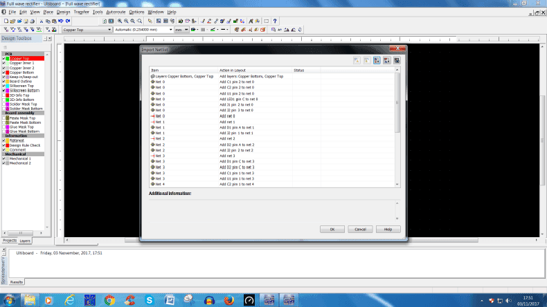
ULTIBOARD 12.0 then saved the file and imported Netlist
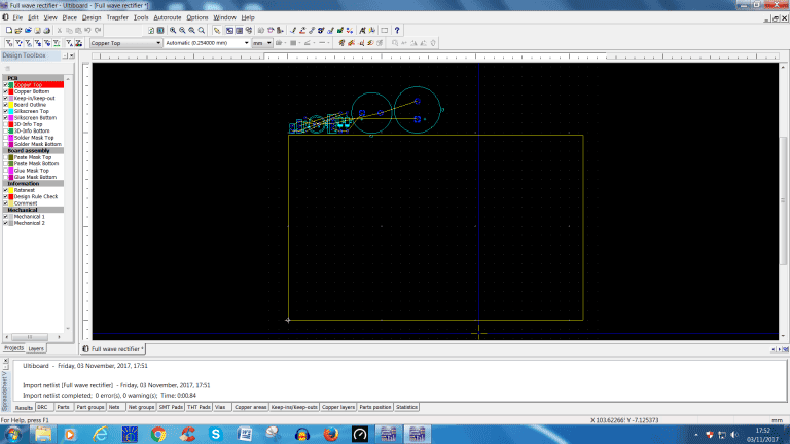
layer for single side PCB with the help of PCB properties icon
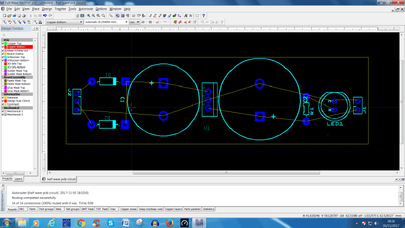
Small PCB after selecting all the components
Design of single-sided PCB layout for full wave rectifier circuit with Multisim software CAD tool was done.
What is Design for PCB Assembly
In the context of PCB assembly, Design for Assembly (DFA) refers to the procedures and factors to maximize the ease of assembly, lower manufacturing costs, and enhance product quality. The following are some DFA guidelines and pointers for PCB assembly.
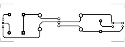
Puzzle Piece Placement
Purpose: To maximize assembly efficiency and minimize trace lengths, strategically arrange the components.
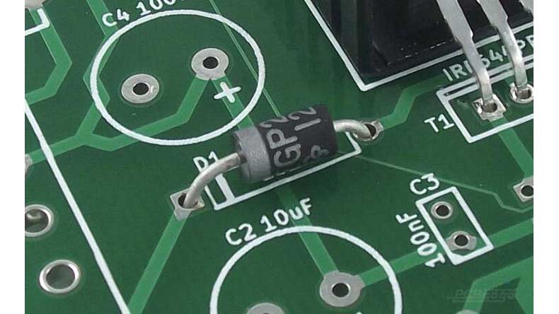
Example: In the example below, Clusters are created by grouping similar components to reduce the distance between related elements. This sensible layout improves PCB design and streamlines the assembly process. Intelligent component placement results in a unified layout that enhances assembly and makes the PCB design more orderly and aesthetically pleasing.
Silkscreen Clarity
Principle: Make sure the PCB has legible and clear silkscreen markings to guarantee accurate component placement throughout the assembly.
Example: The reference designators and values are positioned with consideration in the following image. The PCBA manufacturer is responsible for ensuring correct component identification and placement by reading and defining a silkscreen. Stressing silkscreen clarity will improve component placement accuracy, lower mistake rates, and facilitate a seamless assembly process.
Ensure that reference designators and component values are oriented so that the PCBA manufacturer can easily read them. The text should follow a standard orientation, which is often oriented either horizontally or vertically, and have a legible font size.
Reference designators and values should be placed on the PCB in open spaces away from densely packed areas and components. This lessens the chance of visual congestion and ensures that experts can quickly locate and comprehend the information they need.
Make sure that the values and reference designators correspond to the corresponding component outlines. This visual alignment helps experts assemble components correctly by assisting them in associating the labels with the appropriate parts.
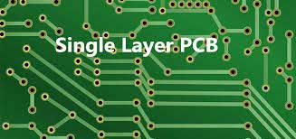
Single-Sided & Double-Sided Assembly
The PCB components are specifically placed on one side in this design. This simplifies the assembling procedure and reduces the production costs associated with double-sided PCBs. Single-sided assembly ensures an easy-to-assemble approach that aligns with a cost-effective strategy, making your PCB design more inexpensive and efficient.
Single-sided construction can be a reasonable and cost-effective choice for smaller circuits or more frugal designs. However, many applications—especially those with more intricate circuitry or specific layout requirements—require double-sided PCBs. Printed circuit boards (PCBs) with two sides offer smaller boards, denser component layouts, and more effective signal routing.
Example: Digital Clock PCB
Double-sided assembly is necessary when creating a PCB for a digital clock to get a compact and feature-rich layout. Time-related functions are managed by the CPU, and components required for the user interface, such as the LED or LCD and time-setting buttons, are located on the top side of the PCB.
The bottom side has vital components for power management as well as other features including a backup battery holder, an RTC module, and passive components. Due to its dual-sided construction, which maximizes space efficiency, the device may accommodate complicated trace routing without compromising its overall dimensions.
Standard Footprint Design
Purpose: Align component footprints with industry standards to ensure compatibility with automated assembly methods.
By following industry norms for component footprints, the PCB design conforms to accepted specifications. One way to guarantee compatibility with automated assembly equipment typically used in the electronics sector is to use standardized footprints such as those advised by the IPC (Association Connecting Electronics Industries). Ensuring component footprints match IPC standards improves the overall manufacturability of your PCB by improving cross-vendor component interchangeability and automating pick-and-place procedures.
Crowding Caution
Purpose: To reduce soldering challenges and ensure a clean, error-free assembly, avoid packing components too closely together.
Example: Moderate component spacing reduces the likelihood of solder bridging during assembly. Enough space around each component encourages precision soldering and lowers the chance of errors. Being attentive while packing your PCB increases its manufacturability, which makes soldering processes easier for machines and yields a more reliable final product.
Trace Routing Optimization
Principle: Incorporate trace routing gracefulness into your PCB design while adhering to industry guidelines for the best possible current flow and signal integrity.
The traces following the suggested standards for width and spacing create a strong current-carrying capability and optimal signal integrity across the circuit. Specific details, such as keeping an acceptable spacing between the traces and the PCB edges, are essential to improve the design.
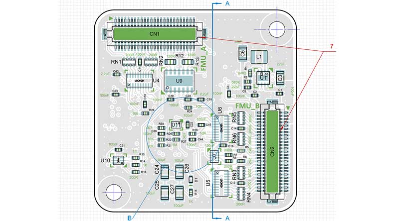
Via Design Strategy
Purpose: To maximize signal integrity and smoothly handle layer transitions.
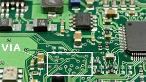
Printed circuit boards require PCB vias as they act as conduits for electrical connections between the board's layers. The design and production of vias are governed by several important factors and regulations.
Via Drilling Rule: The via-drilling rule specifies the drill diameters that are permitted for vias. Designers must specify the minimum and maximum sizes that can be employed based on the manufacturing capabilities and precise requirements of their design.
Via Aspect Ratio: The aspect ratio of a passage may be calculated by dividing its diameter by depth. High aspect ratios, or holes that are larger in diameter than their depth, such as microvias, can make drilling and plating challenging. Maximum aspect ratios are often proposed by design guidelines to ensure manufacturability.
Via Tolerances: Tolerances define the acceptable range for the drilled hole's diameter. Tolerances must be set for the electrical connections made possible by the vias to continue being constant and dependable.
Via Placement: Care must be used while placing vias to preserve signal integrity and avoid interference. Designers need to consider how via placement affects power distribution, signal routing, and overall board functioning.
In the above design, Vias are positioned carefully. These strategically placed vias guarantee a seamless transition between layers, protecting the circuit's integrity and signal quality. You may traverse the complexity of multilayer PCBs by creating a via journey, improving signal performance, and making assembly procedures more effective.
Testing Protocols
Test points in the design are easily accessible and labeled, facilitating a smooth testing process. These sites provide convenient access to diagnostic tools, ensuring efficient testing and debugging processes. When identifying and resolving issues during the testing and assembly phases, the testing protocol saves time and effort.
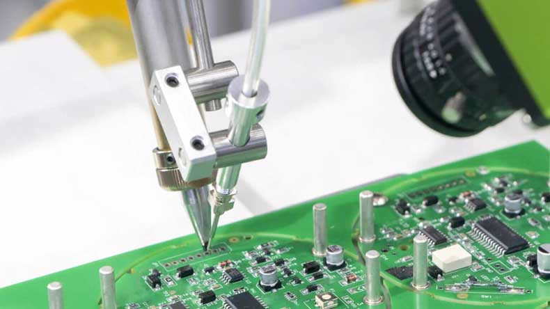
PCB Fabrication and Assembly
Following the Design for Manufacturability (DFM) stage, PCB manufacturing and assembly are essential to bringing our electronic conceptions to life and converting a schematic into a functional device.
PCB fabrication
The process of making printed circuit boards, or PCB fabrication, includes applying a copper layer to a substrate, removing surplus copper selectively to create circuit traces, and adding insulating layers to create a working electronic circuit.
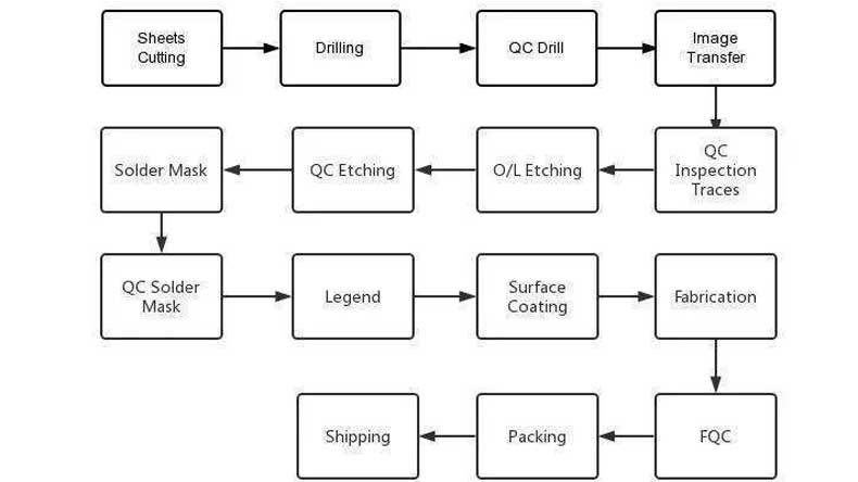
Design: The first step involves creating a thorough schematic that outlines the locations of parts and electrical connections, providing the framework for the construction and functionality of the PCB.
CCL Manufacturing: Copper-clad laminate is a substrate that provides a conductive surface and gives the circuitry's basis.
Inner layer creation: This phase establishes the inner layers of the printed circuit board and provides the framework for building the circuit.
AOI Inspection: To ensure that the circuit design is exact and true, Automated Optical Inspection examines the inner layers for defects or errors.
Lamination: During lamination, the PCB layers are heated and compressed together to create a strong, cohesive board structure.
Drilling: Accurate drilling of holes is necessary to attach components and connect the various circuit parts on the PCB.
Panel Plating: By adding copper plating to the drilled holes in the panel plating, effective electrical connections are made for the board.
Secondary Inspection: A second inspection stage confirms the overall quality of the PCB before moving further with the production process.
Outer Layer Processing: This phase establishes the outer layers of the PCB.
PCB Assembly
The process of integrating electrical components onto a PCB to form a working electronic system is known as printed circuit board assembly, or PCB assembly for short. It entails affixing components like resistors, capacitors, and integrated circuits to pre-designated regions by a blueprint.
Design for Assembly (DFA) Validation
The initial step in the PCB assembly process is the Verification of the Design for Assembly (DFA). To ensure accuracy, a thorough examination of the Gerber/ODB++ files and Bill of Materials (BOM) is necessary at this critical phase. It establishes the foundation for a faultless assembly process.
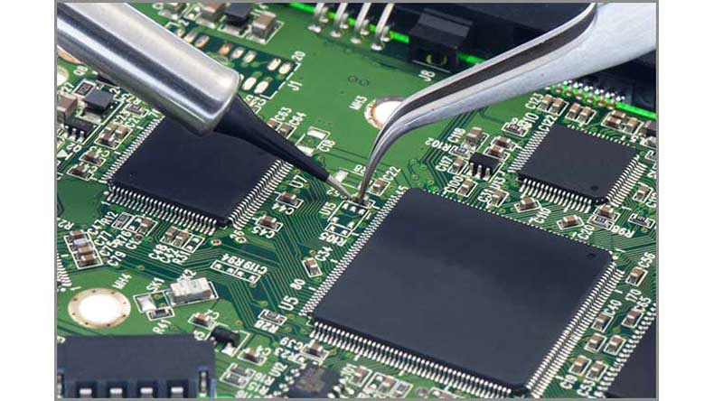
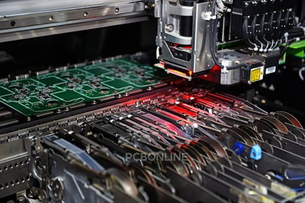
Surface Mount Technology (SMT) Component Placement
Surface Mount Technology (SMT) is the next stage of assembly when electrical components are precisely installed onto the printed circuit board using a pick-and-place machine and soldered by a reflow oven. By the tests including solder paste inspection, X-ray inspection, and AOI, you can be sure that the pieces are positioned precisely for optimal performance.
Through-Hole Component Installation
Through-hole assembly involves installing PTH components by inserting the component pins through the PCB holes and wave soldering. High-requirement PCBA with thermal-sensitive components may require selective soldering instead. By allowing for components that need a different soldering technique, we increase the structural stability of the board.
PCBA Cleansing
After assembly, the boards conduct a thorough cleaning process. It can be ionized water or Plasma cleaning.
Concluding Examination and Testing
Comprehensive testing and inspection are carried out to assess the performance and quality of the PCBAs. They include functional testing, thermal aging, peel strength test, metallographic inspection, application simulation test, etc. The PCBA tests help identify and address any potential issues before the PCBA or final product is delivered.
Conformal Coating
The last step is to apply a protective Conformal Coating. This layer serves as a barrier, keeping the PCBAs safe from outside influences and ensuring their reliability and endurance in real-world applications.
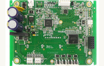
One-Stop PCB Design and Assembly Manufacturer PCBONLINE
PCBONLINE is an EMS (electronic manufacturing service) PCBA supplier that provides PCB design and assembly. You can have PCB, PCBA, and final product designed, manufactured, and assembled by PCBONLINE.

Founded in 1999, it has an R&D team that can design PCBA meeting your specs requirements, two large advanced PCB manufacturing bases, and one PCB assembly factory.
PCBONLINE has successful PCBA examples in PCB design and assembly for consumer, automotive, industrial, computer, communication, defense, and medical electronics.
The R&D team of PCBONLINE has an average of 20 years of experience in PCB design and assembly and can solve technical issues effectively.
Besides PCB design, PCB fabrication, and PCB assembly, PCBONLINE provides PCBA value-added services, including further processing the PCBA to be a system or product, enclosures, and box-build assembly.
For bulky PCBA production, PCBONLINE offers free R&D, samples, and PCBA functional testing.
The PCB fabrication and PCB assembly at PCBONLINE are traceable and certified with ISO 9001:2015, 9001:2016, IATF 16949, RoHS, REACH, UL, and IPC.
Once receiving your question, inquiry, or Gerber and BOM, PCBONLINE will provide you with one-on-one engineering support throughout your journey. To contact PCBONLINE, please send emails to info@pcbonline.com to get a quote.
ConclusionPCB design and assembly are important steps in the production of electronic products. Whether you have designed the PCB or not, you can contact the one-stop and professional PCBA manufacturer PCBONLINE to provide you with assistance and electronic assembly.
PCB assembly at PCBONLINE.pdf