
The Internet of Things (IoT) has already transitioned from a concept to a fundamental pillar of modern industry and daily life. Whether it is a smart home thermostat, an industrial sensor tracking vibrations in a factory, or a wearable medical device, the complexity of these IoT devices requires advanced PCBs (printed circuit boards), including HDI PCBs, rigid-flex PCBs, high-frequency PCBs, and multilayer PCBs. To bring a successful IoT product to market, you need a manufacturing partner that provides reliable IoT assembly services meeting the requirements of connectivity, power efficiency, and miniaturization.
PCBONLINE provides a comprehensive, one-stop IoT assembly solution to take your project from a raw design file to a finished IoT device. By integrating Design for Manufacturing (DFM), PCB fabrication, component sourcing, and final box-build assembly, we provide seamless electronics manufacturing and reduce the time-to-market.
IoT Assembly DFM and PCB Prototypes
Every successful IoT device begins with a solid foundation, DFM, and prototypes. IoT devices are often compact and battery-powered, so the PCB design must be precise and take both manufacturing process feasibility and functions into consideration.
DFM
At PCBONLINE, our service begins with a rigorous DFM check. We not only look at whether the PCB can be made, but also how efficiently it can be made.
Through our DFM, we ensure that Wi-Fi, Bluetooth, or LoRa signals aren't compromised, optimize spacing to prevent shorts in HDI PCBs, and identify hot spots that could affect the lifespan of sensitive IoT sensors. There are many details we take care of in our DFM process. For example, below is how we optimize the IoT shared scooter's motherboard PCB for EMI shielding and testing.
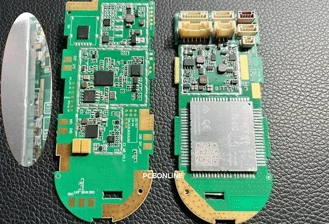
This IoT PCB has components mounted on both sides. On the left of the picture, the components in the middle area will be covered by a metal shielding against EMI. Initially, our customer's PCB design made the EMI shielding cover a surface-mounted metal part directly fixed above the components. But from the picture, you can see that our real PCBA doesn't have it. Instead, our engineers changed our customer's surface-mounted EMI shielding cover design into a snap-latch metal cover. On the real PCBA, there are snap latches mounted. Only when box-build assembly, the metal cover is secured by the snap latches to cover components beneath it.
Why does PCBONLINE change our customers' design? Because our experienced engineers foresee the AOI (automated optical inspection) and X-ray inspection for the components beneath the EMI shielding cover. In the PCB assembly process, if the metal shielding cover is picked and placed, the ICs and other components beneath the cover can't be checked by the AOI machine after reflow soldering. Also, the X-ray machine can't inspect the hidden joints. Instead, through our PCB optimization, both the AOI and X-ray inspections can ensure the IoT product's soldering quality, and the EMI cover also protects the components from EMI.
PCB prototyping
Before jumping into mass production, PCB prototyping allows for functional validation. We offer quick-turn prototypes that mimic the final production quality, allowing engineers to test firmware and hardware compatibility early in the cycle.
There may occur unexpected issues during prototyping, and PCBONLINE has rich experience to solve all of them for a streamlined mass IoT manufacturing and assembly process. For example, below is IC programming for an ESP32 IoT PCBA project during our prototyping process.
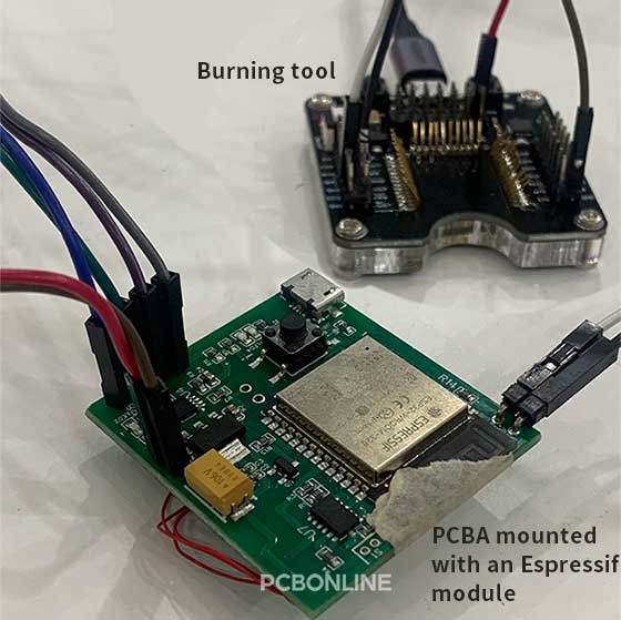
During IC programming for the ESP32, we met an insufficient power supply issue — each time the programming process starts, after a while, there's the "SYNC" error message, indicating insufficient power to function properly. Our engineering team spent two hours testing and troubleshooting, and found the cause: a Cold Boot of the burning tool used for IC programming.
Our engineer quickly came up with the solution: manually removing the GND connection port again and installing the connection twice. Then, the burning program can run successfully!
Advanced PCB Fabrication and Component Sourcing
IoT devices often require specialized materials, such as flexible PCBs for wearables or high-frequency laminates for 5G connectivity.
Custom PCB fabrication
PCBONLINE specializes in various PCB types essential for the IoT ecosystem:
Our engineering team can provide complete PCB R&D services, including:
- Rigid-flex PCBs: Ideal for small form-factor devices like smartwatches.
- HDI PCBs: Necessary for complex IoT gateways that require high-density wiring.
- Metal-core PCBs: Aluminum PCBs and copper-core PCBs are used in high-brightness smart lighting systems to dissipate heat.
- High-frequency PCBs: Low dielectric constant and loss, maintaining signal integrity in RF, high-speed, and microwave applications.
- Ceramic PCBs: Offering the best thermal dissipation and resistance in harsh environments.
Reliable component sourcing
The global electronic component market can be volatile. Our sourcing team leverages a global network of verified suppliers to procure genuine ICs, sensors, and modules. We prioritize traceability, ensuring that every component, from the MCU to the smallest capacitor, meets the required specifications to prevent field failures.
SMT and THT IoT PCB Assembly

PCBONLINE's turnkey PCB assembly factory in Shenzhen provides high-precision SMT (Surface Mount Technology) and THT (through-hole Technology) assembly for IoT devices.
Our PCBA factory has one component warehouse, 4 automated SMT assembly lines, 4 THT assembly lines, 4 post-assembly lines, and comprehensive machines for PCBA value-added services.
Each of our SMT lines is equipped with dual-AOI systems, a lead-free 10-zone reflow oven, and three pick-and-place machines capable of handling the smallest components, such as 01005 chips and fine-pitch BGA packages.
Our THT assembly supports both wave soldering and selective soldering, depending on the thermal sensitivity of your IoT PCB.
Besides SMT and THT assembly, PCBONLINE's IoT assembly services include these value-added services:
- Conformal coating: Many IoT devices operate in harsh environments (outdoors, factories, or near the human body). We apply a protective chemical coating to shield the electronics from moisture, dust, and chemical contaminants.
- IC programming: We offer pre-assembly or post-assembly IC programming, ensuring your proprietary firmware is securely flashed onto the hardware.
- Waterproof encapsulation: If your IoT product has a waterproof requirement, we can encapsulate critical components or even the entire PCBA.
Rigorous Testing and Quality Assurance
An IoT device is only as good as its reliability. A single failure in a smart city sensor network can be costly to repair. Our PCBA tests are already taken during the PCB assembly process, including AOI, X-ray inspection, and first-article inspection. However, after PCB assembly, we also have the PCBA functional testing and burn-in aging on the IoT assembly.
- PCBA functional testing: We develop custom testing fixtures to simulate the IoT device's end-use environment. This ensures that the sensors, communication modules, and power management circuits all work in harmony.
- Burn-in aging: To eliminate early-stage component failure, we perform burn-in aging. By running the PCBs under elevated temperatures and electrical loads for a set duration, we ensure that only the most robust units reach your customers.
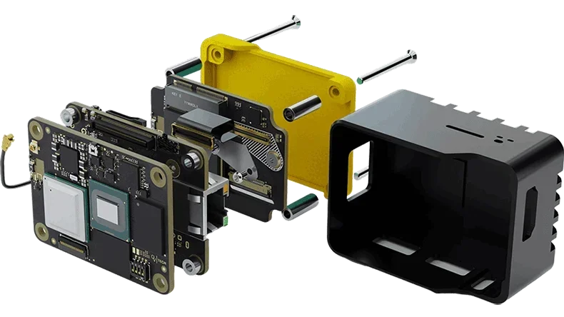
Box-Build Assembly: The Final Step
We go beyond the circuit board to provide a complete mechanical integration. Our box-build assembly includes the enclosures, cabling, final product assembly, and packaging.
- Enclosures: Integration of plastic or metal housings, including custom CNC or injection-molded parts.
- Cabling & harnessing: Installation of internal wiring, connectors, and antennas.
- Final assembly: Mounting the PCBA into the housing and sealing the unit.
- Packaging: Retail-ready packaging, labeling, and kitting with manuals and accessories.
By choosing our box-build service, you eliminate the logistical nightmare of coordinating between a PCB fabricator, an assembly house, and a mechanical molder. We handle the entire bill of materials (BOM), providing a single point of accountability.
Partner with PCBONLINE for IoT Assembly Service
PCBONLINE is a turnkey PCBA manufacturer providing IoT assembly service. We provide all the electronics manufacturing and materials used for our IoT PCB box-build assembly services, including the enclosures.
Our IoT assembly services offer:
- Complete procurement: We source and customize enclosures, cables, and accessories from reliable suppliers.
- Engineering support: We check enclosure and accessory designs for compatibility with your PCBA and can suggest design changes.
- Free DFM/DFT: We provide free Design for Manufacturability (DFM) and Design for Testability (DFT) checks to ensure that designs are optimized for a smooth production process.
- Special capabilities: IPX8 waterproof enclosures and encapsulation for rugged outdoor devices.
- Quality assurance: IPC-A-610 Class 3, automotive-grade or industrial-grade inspection standards.
- Turnkey delivery: From PCB fabrication to final product packaging and shipping.
- Testing and value-added services: Offering a range of quality assurance services, including X-ray inspection for hidden-joint PCBAs, first-article inspection, PCBA functional testing (FCT), IC programming, burn-in test, PCBA coating, enclosures, and box-build assembly.
Founded in 2005, our two advanced PCB manufacturing bases are in Jiangsu and Jiangxi Provinces, and our turnkey PCB assembly factory is in Shenzhen. Besides, we have an R&D team and a global supply network. We also maintain strategic cooperation with the top 3 fixture and enclosure factories in China to manufacture the custom PCBA fixtures and device enclosures.
PCBONLINE manufactures, assembles, and tests PCBs and PCBAs to box builds as a source factory manufacturer under one roof, from prototypes to bulky production, saving costs and time for you.
We keep strategic cooperation with the top 3 enclosure manufacturers in China to manufacture custom device enclosures.
We can design the PCB enclosure to match your PCB. Besides, we can help create user manuals, installation guides, and compliance labels.
Our high-quality PCBA contract manufacturing is certified with ISO 9001:2015, ISO 14001:2015, IATF 16949:2016, RoHS, REACH, UL, and IPC-A-610 Class 2/3.
Our one-on-one free and professional DFM helps you debug and improve design, to ensure the manufacturability, cost-effectiveness, and final device success.
Whether you need EMS PCB assembly to build consumer IoT devices, creative electronic products, automotive/medical-grade systems, etc, with 20 years of PCBA manufacturing and box build experience, we ensure that both electronics performance and final product presentation meet the highest standards. To get a quote for your IoT assembly project, email us at info@pcbonline.com.
Conclusion
From the initial DFM review to the final box-build and shipping, PCBONLINE is committed to turning your IoT vision into a high-performance reality. Contact us to build IoT devices for success from prototypes to mass production.


