
This PCB soldering guide explains what is PCB and prototype, the steps in PCB soldering, PCB soldering tips, and precautions.
1. Brief Introduction of Soldering:
Soldering is the process of joining two or more metals by melting the solder to make connections.
Solder is basically a low melting alloy generally we used tin-lead.
The metals to be soldered are heated with a soldering gun at a specific temperature and then solder is melted into the connection.
PCB boards are used for the electrical connection of electronic or electrical components.
Soldering is used for the permanent connection of electrical components.
Our main focus is on PCB soldering.
PCB soldering
PCB soldering is basically mechanical supports and electrical connections of electronic or electrical components using the conductive path.
Usually, we use PCB for small projects. PCB soldering is very easy below we detailed a discussion on PCB soldering so a new one can do this with ease.
2. Components Required for PCB Soldering:
- PCB board
- PCB layout (on software)
- Soldering gun
- Wirecutter
- Wire stripper
- Solder sucker
- Solder wire
Below are brief descriptions of the components.
PCB board
Printed circuit boards (PCB) are very important to electronic gadgets which can be used in industrial as well as for domestic purposes.
PCB boards are used for the electrical connection of electronic or electrical components.
Different sizes of PCB boards are available we select according to our circuit design.
PCB Layout
![]()
PCB layout can be used to design electronic circuits.
Basically, we made the layout/design on software.
This PCB design is pasted on the PCB board for the connections of electronic components.
Soldering gun
A soldering gun is used for electrical connections.
We use it for soldering the solder, where we needed more heat to melt. Soldering guns have a rating of about 240 watts of power.
In the PCB circuit, it is used to make the connection of wires on the boards.
![]()
The soldering gun is heated at a temperature where our solder wire becomes a thick fluid then we start soldering on the PCB design.
With the solder gun, we generally connect electronic components and paths of electrical connections.
Wire cutters and strippers:
![]()
Wire cutters used where we have to remove the insulation of electrical wires in order to make connections.
While the wire strippers having an opposing blade having a notch at the middle of the blades where the wire is being placed.
The strippers are rotated around the wire, and the outer insulation comes off leaving the actual wire intact.
Generally in PCB boards, we use them to cut the solder or the leads of electronic components to make the circuit board clean.
Solder sucker
We use a solder sucker to remove the electronic components from the PCB board.
When a wrong component unintentionally is pasted on the PCB board with a soldering gun we use a sucker to remove it.
When our connections on the PCB boards become short during soldering we use a sucker to remove the soldering to make the circuit safe and good connections.
Solder wire
Solder is a fusible metal alloy that is used to produce a strong connection between metal workpieces.
The solder is then melted in order to connect the pieces of the components on PCB boards after cooling, which requires that metal alloy for use as a solder have a small melting point than the pieces being connected.
After PCB designing we use solder to connect the components on the board and for electrical connection the path where voltage or current will flow.
3. Step by Step Guidance to PCB Soldering
Below we are going to discuss the steps followed in PCB soldering
Step 1: PCB design and its output:
PCB layout is made on PCB design software commonly use OrCAD, Pads, or KiCad.
The design of products is a scheme design that has to be carried out the basic module of the circuit design, then the diagram is fully drawn, all of which can be completed manually.
Then a design will be applied to indicate the PCB design process.
Once the PCB design is completed fully for production, then export the design into the format their user can ask for.
After fully examining the design, then forward PCB files to PCB Board for production.
To make sure that the design meets the requirements fully with the small tolerance during the production process, almost all the PCB production units run the design for production, and then check the circuit board's fabrication.
Step 2: From the Software Files to Film
After the completion of the design output, the second step is to paste the files onto the PCB boards.
Manufacturers use a special printer known as a plotter, that makes the photo films of the PCB, to print the PCB boards.
We use the films to image the printed circuit boards.
Basically, it is a type of laser that prints the design.
Plotters use an accurate printing process to provide complete detail of the film of the PCB design.
The end product is a plastic sheet with a photo of the PCB boards with black ink. The inner layers show a conductive copper path while the remaining shows non-conductive.
Step3: Prepare the Iron and Surface
When the PCB files are pasted fully on the PCB boards then you need to prepare the iron used for soldering and clean the Surface of the PCB boards.
Make sure that no dust or other particles are on the PCB boards.
Before using an iron you need to complete the process of tinning.
This process is coating the tip of the solder with iron to avoid the heat transfer process.
Once the iron is completely heated, coat the tip with solder and make sure that the entire tip is a cover-up.
For good soldering, you need to clean the PCB board and use an industrial pad to wipe the surface clean of any dust and debris.
We use acetone cleaner to give it an additional wipe-down.
Or we use a brush to clean the dust particles on the PCB boards.
Step 4: Place the Components:
Now you need to place the components on the PCB board as already indicated on the board by the PCB layout you pasted on it.
By placing all the electronic components on the boards where they belong then bending the leads of components into the holes given in the board.
Ensure that all the components are being placed correctly any wrong placement may cause damage to the circuit.
So check the circuit components before soldering.
Step5: Heating:
Now apply heat with solder to the tip of the iron.
For the proper joint hold the iron so the tip touches both the board and the component lead.
Once the tip is in position, the solder you may apply will make contact with both the lead and the board, heating them up and preparing them for soldering.
If you notice the area starts bubbling during heat remove the heat immediately.
Wait for it to cool and then heat it again, more carefully.
Step6: Add Solder at the Joint
Once you heat the joint then you need to solder at you made on PCB boards.
By touching the tip of the solder, to solder the pad and lead as shown in the example below. If you heated the space correctly the solder should flow freely and flux should begin to liquefy and bubble.
Keep adding the solder around the joint until it is entirely coated.
After completing the solder remove your iron from the area.
As the joint cools down make sure it stays absolutely still.
Make sure that all joints and all components are soldered carefully, in the case when any joint or component is not soldered or has loose soldering, solder it again so that a good and safe circuit would be made.
Step7: Cleanup the Joint
After the cooling of the joint conduct a small inspection of the whole PC circuit.
If the solder joint looks good then you need to trim the leads of the components.
We need cutters to cut the leads of components.
We cut the leads from the top of the joint of all the components step by step.
After trimming of leads make sure to clean up the extra flux on the board making it a clean product.
Use a brush to make clean the PCB boards so that no piece of iron or any other thing would remain.
4. Tips and Precautions
Soldering needs practice.
But if you are a new one then take care of the following tip and precautions.
Here we are going to discuss some tips for soldering.
- Must use Heat sinks for sensitive components like leads of ICs and transistors.
- Keep the iron tip clean for better conduction and joint. Can use a wet sponge to clean the tip between joints of PCB boards.
- Inspect the joint carefully and use devices like an ohmmeter to check the resistance of the components.
- Install the sensitive components of soldering at the end to reduce the damage during the assembly of parts.
- Try to avoid breathing the smoke created where you are working to prevent the buildup of noxious fumes.
Now we discussing the precautions during PCB soldering.
- During heating, the solder gun is heated up to a high temperature which may burn the skin try not to touch the solder gun, solder, and the PCB board where the solder is pasted.
- Use stands for the soldering gun, after soldering put the gun at the stand so the soldering gun will not touch you are any other things. Otherwise, it may cause burning.
- During soldering keep your face at some height above the joint because toxic fumes from the flux of the solder and other coatings will be harmful to your respiratory system and to the eyes.
How to Find a Reliable PCBA Supplier?
Are you looking for a reliable manufacturer to provide you with the best PCB and PCBA at a reasonable price? PCBONLINE is a one-stop company that can meet all of your demands. They are good at producing and assembling all kinds of PCBs, their service won't let you down.
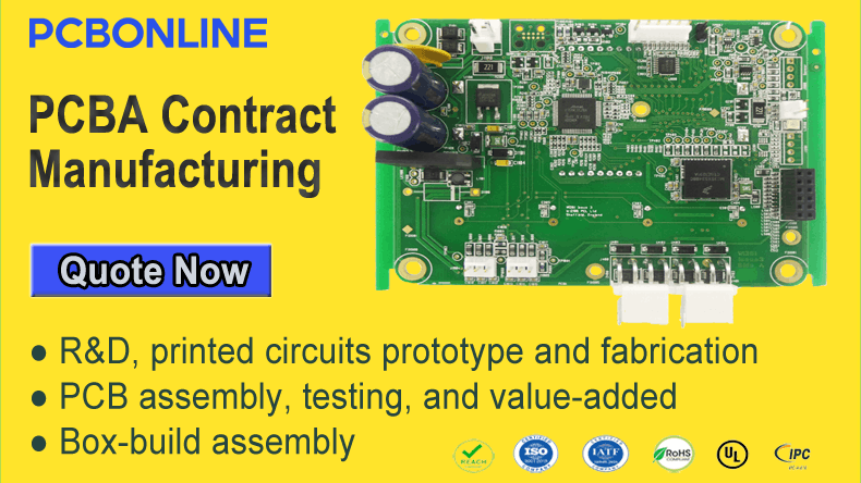
- PCBONLINE provides various assembly solutions including low volume, medium volume, high volume, consigned, turnkey, and SMT and THT PCB assembly.
- PCBONLINE can assemble your PCB as fast as 24 hours perfectly tailored to your business needs.
- ISO9001:2015 international standard quality management system will bring out the best assembly quality.
- Advanced machines and technology are used, such as 30 Panasonic and Yamaha SMT lines, Germany ERSA selective wave soldering, solder paste detection 3DSPI, AOI, X-ray, etc.
- All of the operation engineers have more than 10 years of PCB assembly experience.
Conclusion
Printed circuit boards perform an important part in digital and electronic devices these days. PCB design and its layout form an essential part of the design of the product. PCB helps the digital electronic devices and their wiring through the surface is really remarkable. From the above discussion on PCB soldering, the step-by-step guidance, tips and precautions, and online services that we are providing you, we concluded that no one can feel any type of difficulty with PCB soldering if he/she wants to make the PCB projects on his behalf. Now it's the era of online services that makes life much easier a person cannot feel any kind of problem in any of his tasks. Our online service provides you with a quick and easier way of soldering. This service has all the tools that are needed to create a clean and solid design.


