
Question: Having PCB solder failure. Looks like the PCB pad is damaged but not sure of that. Would I need to replace that PCB pad?
What issue is with your PCB? To help you better comprehend and maintain a strategic distance from the possible blunders in your printed circuit board plans, we've accumulated top-notch of the most well-known PCB issues experienced in PCB fabrication. You can know why they happen and how to repair PCB pads or PCBs in this article.
![]()
PCB Pad Issue: Burnt PCB Pads
The high temperatures utilized during the circuit board fabricating interaction can wear out segments of the PCB, particularly if the segments are loaded firmly along with little space encompassing them. This plan traps warmth and builds the danger of overheated and worn-out circuit boards. Consumed circuit boards are especially precarious to manage because the warmth inside the board is probably going to annihilate the defective part alongside numerous others, making analysis unimaginable and delivering the board all-time unusable.
Solution:
Either you find a reliable PCB company - PCBONLINE so that these issues never happen, or you have to repair the burnt PCB pad by hand. You cut the burnt part as little as possible to a good track, remove the burnt pad, use a small copper foil to overlap the original pad and solder the joint with the track, pierce the hole, solder the component, and finally trim the repair. However, this rescue may affect the circuit's resistance and performance.
![]()
PCB Issue 1: Plating Voids
Plating voids happen at what stage? First, let's see the normal workflow.
Plated through openings are copper-covered openings in a printed circuit board. These openings permit power to be conveyed from one side of the circuit board to the next. To make these openings, the PCB fabricator drills openings through the circuit board, penetrating the material right through. A layer of copper is then added to the surface of the material along with the dividers of these openings through an electroplating interaction. This cycle stores a slim layer of electroless copper onto the circuit board in an interaction called deposition. After this progression, additional layers of copper are added and scratched to make the circuit.
These plating voids happen because, for some explanation, the material is not covered equally during the affidavit interaction. The explanations behind this incorporate pollution of the material, air bubbles trapped in the material, inadequate cleaning of the openings, lack of catalyzation of the copper in the statement cycle, or unpleasant opening boring. Any of these issues can bring about plating voids along with the dividers of the circuit openings.
![]()
Solution:
There is no so-called "remedy" to the board once the plating voids happen. This issue can only be prevented from the PCB manufacturing side. Deformities because of defilement, air bubbles, or deficient cleaning can be evaded by cleaning the material appropriately in the wake of penetrating. Manufacturers should use an appropriate number of high-speed drills to avoid crushing materials, so that rough surfaces will not be formed, resulting in plating voids. Work with a reliable PCB manufacturer - PCBONLINE and you will never worry about any PCB issues.
PCB Issue 2: Acid Traps
The acid trap is the basic term for intense points in a circuit. They allude to this way because these intense points trap acid during the PCB scratching measure, permitting the acid to develop in the alcove of the point. The point practically saves the acid in the corner for a more drawn-out period than the plan calls for, making the acid consume more than proposed. Subsequently, the acid can bargain an association, making the circuit deficient and causing more major issues later.
Most creators know about the issues brought about by intense points in a circuit board and are along these lines prepared to stay away from them. In any case, mistakes do occur. Frequently, intense points are the consequence of straightforward human mistakes, but some plan programming projects may likewise set circuits to intense points if the settings are not appropriately changed.
Solution:
Once acid traps happen, you cannot rescue them anymore. But the issue can be avoided. Here is a way to prevent this - when assembling the board, you or your manufacturer use non-conductive epoxy resin or apply solder resist on the hole.
PCB Issue 3: Starved Thermals
Thermals are little encompassing pads and are utilized to interface pads to the plane. These thermals permit the pads to be all the more successful in scattering heat and are significant parts during the soldering cycle. Once in a while, in any case, voids between the warm and the remainder of the plane, or the warm and the pad, can bring about a fragmented association, decreasing the viability of the warmth move framework these thermals make. This can bring about a few practical issues.
The wellspring of this issue is frequently in the assembling. These warm associations are generally tied accurately to a plane layer in a CAD framework, however, they are one way or another fabricated with a decreased association with the remainder of the plane. Assembling issues during warm trim or machining, for example, over-machining or inappropriate embellishment, would all be able to bring about this issue, and can regularly be cured by supplanting the warm.
Solution:
The key to fixing the starved thermal issue is spreading the heat as much as possible. You can install fans or heat sinks to transfer heat from the circuit board, but small-sized devices cannot install these devices. In this case, you can use thicker copper for high current, or you can place high-current electronic components like a microcontroller in the center of the circuit board when designing the circuit, or you can apply a thicker circuit board. Below is an image of a high-quality thick-copper PCB for your reference.
![]()
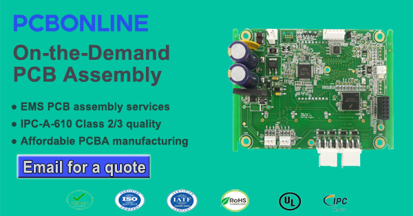
How to Avoid Annoying PCB and Pad Issues - Work with PCBONLINE
Yes, work with PCBONLINE. As a profoundly appraised producing organization, we can recognize such flaws effectively and prevent them. The PCB or pad issues never get an opportunity to mess up the circuit board. We offer free samples for batch production, PCBA functional testing, and design for excellence.
Layer: 1 ~ 42
Laminate: normal Tg/high-Tg/lead-free/halogen-free
Surface finish: OSP/HASL/LF HASL/ENIG/immersion tin/immersion silver/carbon ink
Board thickness: 0.15mm ~ 3.2 mm
Max board size: 500mm × 580 mm
Copper thickness: (inner finish copper) 1oz-4oz, (outer finish copper) 1oz-7oz
Min. line width/spacing: 0.0635mm/0.0635mm
Min. CNC drilling size: 0.15mm
Min. laser drilling size: 0.075mm
HDI stack up: 1+N+1, 2+N+2, 3+N+3
PCBONLINE manufactures high-quality PCB and PCBA without any PCB pad issues or other. You can contact info@pcbonline.com to get a quotation.


