
As printed circuit boards (PCBs) are getting smaller, faster, and more complex, using advanced via structures to make HDI PCBs is the trend. Among the advanced PCB vias, blind vias play a critical role in high-density interconnect PCB designs.
PCBONLINE is a one-stop blind via PCB manufacturer providing HDI structures from 1+N+1 to 4+N+4. Our article explains what a blind via is, how it compares with other via types, and how to manage blind via PCB thermal performance effectively.
In this article:
Part 1: What is PCB Blind Via Part 2: Blind Via vs Buried Via vs Microvia Part 3: Thermal Management of Blind Via PCB Part 4: Order Blind Via HDI PCB 1+N+1 to 4+N+4 from PCBONLINEPart 1: What is PCB Blind Via
In an HDI PCB, a blind via electrically connects an outer layer (top or bottom) to one or more inner layers. It does not pass through the entire PCB.
In simple words, a blind via:
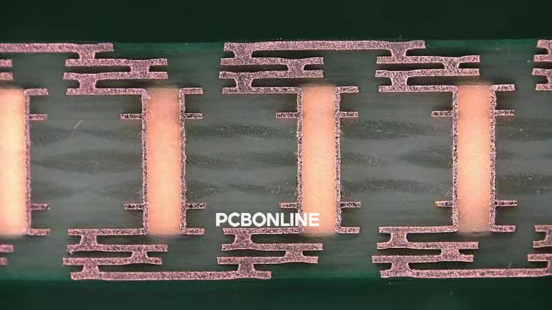
![]()
- Starts on the surface.
- Stops at a specific internal layer.
- Does not go all the way through.
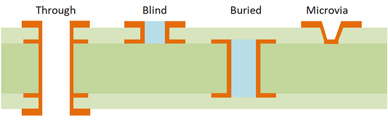
This is different from traditional through-hole vias, which connect all layers from top to bottom.
Why Blind Vias Are Used
Blind vias are mainly used in HDI PCB designs where space is limited. As electronic components become smaller and pin counts increase, routing all signals with traditional vias becomes inefficient or even impossible.
Blind vias:
- Save routing space on inner layers
- Stops at a specific internal layer.
- Enable higher component density
- Improve signal integrity
Blind via design considerations
- Blind vias increase manufacturing complexity and cost.
- Buried vias require multiple lamination cycles.
- Microvias demand precise laser drilling and plating control.
How Blind Vias Are Manufactured
Blind vias are created using controlled-depth drilling or laser drilling.
Mechanical drilling is used for larger blind vias.
Laser drilling is used for micro blind vias in HDI designs.
After drilling, the vias are plated with copper to create electrical conductivity.
Applications of Blind Vias
Blind vias are widely used in:
- Smartphones and tablets
- Wearable devices
- Automotive electronics
- Servers and data center hardware
- Medical electronic devices
These applications demand compact size, high performance, and reliability. Blind via PCBs perfectly meet their requirements.
Part 2. Blind Via vs Buried Via vs Microvia
To fully understand blind vias, it is important to compare them with other via types: buried vias and microvias.
Blind Via
- Connects the outer layer to the inner layer
- Visible from one side of the PCB
- Does not pass through the entire PCB
- Used in HDI designs for surface routing optimization
Buried Via
- Connects only internal layers
- Not visible from the outside
- Fully enclosed within the PCB
- Used to free up outer-layer routing space
Microvia
Microvias are a subset of blind vias but with much smaller dimensions.
- Less than 150 microns in diameter
- Created using laser drilling
- Usually connects adjacent layers (e.g., Layer 1 to Layer 2)

Microvias can be blind microvias, stacked microvias, and staggered microvias.
In HDI PCB design, combinations of blind vias and blind are often used together to achieve optimal performance and density.
Blind Via vs Buried via vs Microvia
|
Feature
|
Blind via
|
Buried via
|
Microvia
|
|
Location
|
Outer to inner
|
Inner to inner
|
Outer to adjacent inner
|
|
Visibility
|
Visible on one side
|
Invisible
|
Visible (if blind)
|
|
Size
|
Medium
|
Medium
|
Very small
|
|
Process
|
Mechanical or laser
|
Mechanical
|
Laser only
|
|
Use case
|
HDI routing
|
Inner layer optimization
|
High-density HDI
|
Thermal Management of Blind Via PCB
Blind via PCB thermal management is critical. Because blind vias do not go all the way through the PCB, the thermal dissipation path is restricted. To increase thermal dissipation of blind via PCBs, copper filling with stacked via design is the most common thermal management solution. Other methods include via-in-pad and thermal via array.
1. Copper Filling
Copper-filled vias are one of the most effective solutions for heat transfer. It is widely used in high-power and high-frequency designs.
The via is completely filled with copper instead of air or resin.
Copper has high thermal conductivity.
Heat can move efficiently through the via to the inner layers.
2. Via-in-Pad
Via-in-pad means the via is placed directly inside the component pad. Its benefits include:
- Shorter thermal path
- Improved heat transfer from components
- Better electrical performance
However, vias-in-pad require Via filling (usually copper or conductive epoxy).
3. Stacked Vias
Stacked vias are vertically aligned vias connecting multiple layers.
Stacked vias allow direct vertical heat conduction and reduce thermal resistance.
When combined with copper filling, stacked vias provide excellent thermal performance.
Copper-filled stacked vias are the most common thermal solution in HDI PCBs.
4. Thermal Via Array
A thermal via array consists of multiple vias placed under heat-generating components. It:
- Distributes heat across a larger area
- Transfers heat to the inner copper planes
Thermal via arrays are commonly used under power ICs, CPUs, and LEDs.
Internal Plane Connection
During the layout phase, blind vias should be connected to large internal reference planes, especially ground planes.
Internal copper layers act as heat sinks, absorbing and distributing heat throughout the PCB.
Internal plane connection provides efficient heat spreading and reduced thermal resistance.
How about practices for thermal design of blind via PCBs?
- Use copper-filled vias whenever possible
- Combine stacked vias with copper filling
- Place thermal via arrays under high-power components
- Connect vias to ground planes or power planes
- Avoid isolated vias that trap heat
When you design the layout, avoid these mistakes!
- Using hollow vias in high-power areas
- Poor connection to internal planes
- Insufficient via density
- Ignoring thermal simulation during design
Proper thermal design ensures long-term reliability and stable performance.
Order Blind Via HDI PCB 1+N+1 to 4+N+4 from PCBONLINE
When designing advanced PCBs, choosing the right manufacturing partner is essential. PCBONLINE provides one-stop services for the blind via HDI PCB fabrication and assembly.

We make HDI layer structures from 1+N+1 to 4+N+4.
- 1+N+1: One HDI layer on each side of a core
- 2+N+2: Two HDI layers on each side
- 3+N+3 / 4+N+4: More complex multi-layer HDI structures
As the number increases, routing density improves, design flexibility increases, and manufacturing complexity increases. However, PCBONLINE has sufficient capabilities to solve all HDI manufacturing issues.
Founded in 2005, PBONLINE has two large advanced PCB manufacturing bases and one PCB assembly factory.
PCBONLINE supports laser-drilled microvias, blind and buried vias, stacked and staggered via structures, and copper-filled vias.
We support high-layer count HDI PCBs up to 64.
We provide a one-stop blind via HDI PCB manufacturing, including component sourcing, PCB fabrication, assembly, testing, and system integration.
SMT assembly with fine-pitch BGA placement accuracy and custom reflow profiles for warpage-free soldering.
PCBONLINE offers one-on-one engineering support, including stack-up design recommendations, via structure optimization, thermal management guidance, and DFM checks.
Our capabilities are suitable for high-speed communication devices, automotive control systems, industrial electronics, and medical devices.
High-quality HDI PCBA manufacturing certified with ISO 9001:2015, ISO 14001:2015, IATF 16949:2016, RoHS, REACH, UL, and IPC-A-610 Class 2/3.
Apart from strong HDI manufacturing capability and reliable quality control, we offer fast turnaround time and technical support for complex designs. If you feel interested in blind via PCBs from PCBONLINE, send your inquiry by email to info@pcbonline.com.
Conclusion
Contact PCBONLINE to order a blind via HDI PCB. We are looking forward to your Gerber files, drill files, stack-up details, via structure requirements, and material specifications.
PCB assembly at PCBONLINE.pdf
PCB fabrication at PCBONLINE.pdf


