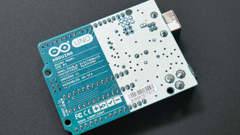
 PCBA is a printed circuit board assembly. It is an electronic mainboard or module created by soldering components on a blank PCB.A blank PCB consists of insulating material sheets, copper foil, and solder masks. When the PCB is soldered with desired components and passes inspections, it is a PCBA.The following is what this article reveals details of PCBA:
Part 1: What is a PCBA?
PCBA or Printed Circuit Board Assembly is a term that refers to circuit boards surface mounted and/or through-hole mounted with electronic components, such as capacitors, resistors, and ICs. Some PCBAs can embed components, such as LTCC ceramic PCBs. LTCC ceramic PCBs.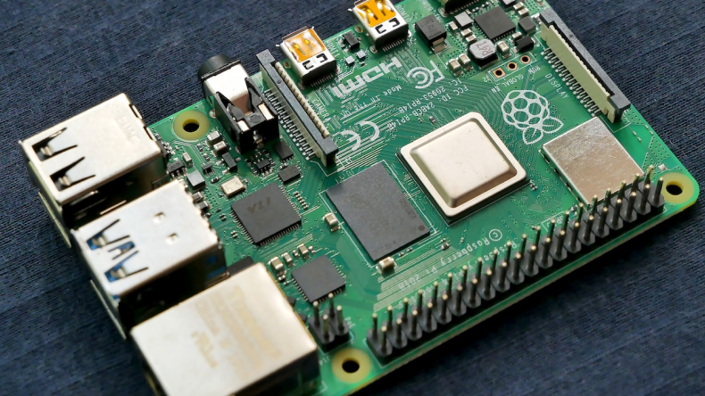 A PCBA includes a PCB and components. A PCB uses conductive traces and pads that are etched from copper layers, which are laminated between the sheet layers that are non-conductive. The components are soldered on the PCB to connect electrically and mechanically.To ensure that the connection between the PCB and components works adequately, solder is welded or inserted into a blank circuit board and inspected to test its performance.You can imagine a PCBA as a cake. Non-conductive layers are the bread, the copper layers between are cream, the solder mask is the chocolate shell, and the components are the fruit and decoration on the top.However, a PCBA is more complex, as copper traces in different layers are interconnected by copper-filled holes, and PCB pads are not covered by solder masks but by a surface finish. Besides, a PCBA can have dual component-mounting sides.
 A PCBA is a semi-electrical product for everything, from a small LED light to a large industrial control system. When PCBAs are installed with enclosures, they are box builds or end products.
Part 2: How do You Get a Custom PCBA

Step1.The first step in designing a custom PCB is in creating a schematic view.The required component is placed on a canvas and their pins are connected with lines that represent the electrical connections. The components usually are taken from a component library which is a part of the design software.There may be multiple variations of the same components depending upon the type of package being used e.g. dual inline package or a surface-mounted chip. The packages may seem the same in the schematic view but are very different in the layout view where the board is actually designed.Apart from the components and their electrical connections, power and ground signals are also needed. Also, connectors have to be placed on the PCB to make a place for power and ground. The board is also required to be connected to external devices, such as potentiometers and LEDs, etc.
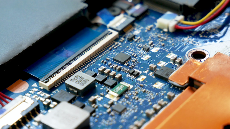
Step2.Once everything is placed in its place, an electric rule check is run to ensure no evident faults.These may include breaks in wires or connections or any missing connection to ground or power etc.Once the schematic is done, the board layout view is checked.
Step3.The components are moved to proper places that make good sense.
Step4.For the board production, signals are assigned to each layer and varying signals on a single layer cannot touch.
Step5.After the signals are laid, a design rule check needs to run to ensure the proper placement of holes, traces, etc. These rules can be customized as well.
Step6.If the design is approved, the design files can be uploaded.The communication language of PCB fabrication is a Gerber file. Each board has multiple files, one for each layer. Another file known as the drill file is used to define where holes need to be drilled.
Step7.Go to PCBONLINE's online quotation system and click Browse Files to upload Gerber.When the Gerber is uploaded, it will run its own error check procedure. It produces an image file of the PCB. You'll need to enter the PCB quantity you want.
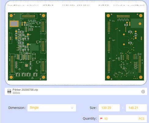
Step8.Check PCB specifications, choose the lead time, and click Buy Now. Follow the next on-screen instructions. After that, it will take half an hour for PCBONLINE to audit your inquiry. Later, PCBONLINE will send an email to notify you about the order. You can send your bill of materials (BOM) and pick-and-place file to info@pcbonline.com for PCB assembly.


