
The reflow soldering process is the most important step in surface mount technology (SMT) assembly to mount surface mount devices (SMDs) onto a printed circuit board (PCB). Reflow soldering is a process where solder paste melts and forms permanent electrical and mechanical connections between the SMDs and the PCB's copper pads. The success of reflow soldering relies on solder paste application, reflow profiling, and design for manufacturability (DFM).
PCBONLIN, an OEM PCB manufacturer providing turnkey PCBA manufacturing, has rich experience in reflow temperature control, SMT stencil design, and DFM. In this article, we will detail how to ensure the success of a reflow soldering process.
Understanding a Reflow Soldering Process
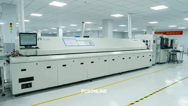
A reflow soldering process is completed in a conveyor-based oven, where the PCB passes through 8 to 12 temperature zones to control the temperature gradient. The hot winds flow perpendicular to the PCB surface, and there's also a weak air draft that flows parallel to the conveyor direction.
At PCBONLINE, our reflow ovens are lead-free with 12 temperature zones, which are the highest manufacturing level in PCB assembly services. The reflow cycle includes four stages: pre-heat, soak, reflow, and cooling.
Preheat
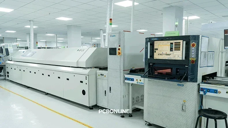
On each of the four SMT lines at PCBONLINE, the PCBs are soldered following solder paste printing, solder paste inspection, component placements, dual automated optical inspections (AOI), and reflow soldering.
After component placement onto the PCB and pre-reflow AOI, the PCB enters the reflow oven and is gradually heated from ambient temperature.
Preheating aims to bring the PCB to a stable temperature and evaporate water from the solder paste. The flux from the solder paste can improve soldering.
During preheating, the ramp-up rate must be carefully managed, limited to 1°C to 3°C. Otherwise, a too-fast ramp-up can induce thermal shock, leading to component cracking or damage to the PCB laminate, especially ceramic PCBs.
![]()
Soak/thermal equilibration
The temperature rise slows down, allowing the PCB assembly to soak at a stable intermediate temperature. Soaking allows temperature equalization across the PCB, minimizing the thermal gradient between large SMDs and small ones.
The soaking stage also activates the flux within the solder paste, which cleans the metallic surfaces (pads and component leads) by removing oxides and improving soldering.
During soaking, the temperature is held below the melting point of the solder alloy. For common lead-free alloys like SAC305 with the melting point of 217°C, the soaking temperatures are often set between 150°C and 180°C.
Reflow zone (time above liquidus)
The temperature is rapidly increased past the melting point (liquidus) of the solder alloy. The hot air melts the solder paste, allowing the liquid solder to wet the SMD component leads and PCB pads. The molten solder is drawn by surface tension forces, resulting in the self-alignment of components.
During reflow, the peak temperature must be high enough to ensure proper wetting, usually(10°C to 25°C above the liquidus temperature.
Besides, the time above liquidus must be sufficient to form the desired intermetallic compound (IMC) layer but limited between 30s and 90s to prevent excessive component and PCB degradation.
Cooling
The assembly is cooled rapidly once it exits the peak temperature zone. At the end of the reflow soldering process, between the PCB and SMD components form reliable solder joints, and we call the board a PCBA (printed circuit board assembly).
Cooling solidifies the molten solder quickly, ensuring a fine-grained crystalline structure in the solder joint for maximum strength and reliability.
During this stage, the cooling rate should ideally be >3°C. Slow cooling can lead to a coarse-grain structure, potentially resulting in brittle or unreliable solder joints.
How to Ensure Reflow Soldering Success
Achieving consistent, zero-defect reflow soldering requires attention to detail in design, material handling, and process management. PCBONLINE has rich experience in PCB assembly, and we pay attention to every detail to provide a successful reflow soldering process.
1. Precise reflow profile
The temperatures in the reflow soldering process follow a reflow profile, which is the blueprint for a successful reflow.
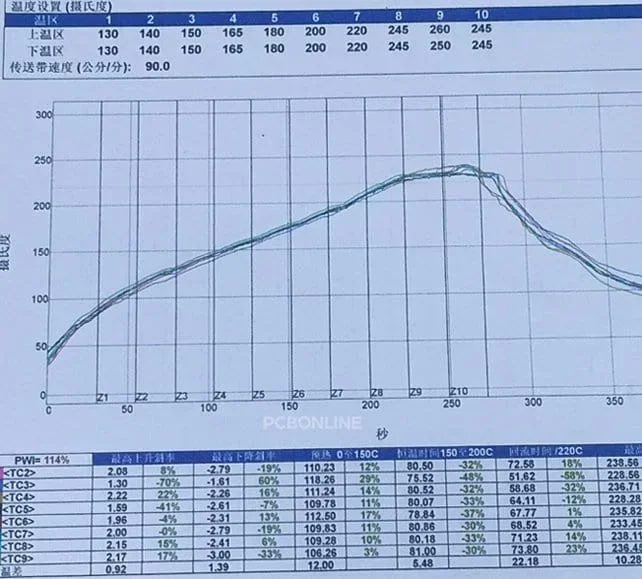
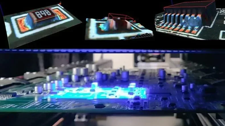
- Profile verification: Use a thermal profiler with thermocouples to attach directly to the PCB to map the actual temperatures experienced by various points on the PCB, especially near large components.
- Zone tuning: Adjust the heater settings and conveyor speed until the measured profile strictly complies with the specifications of the solder paste and the most sensitive components.
- Oxygen control (nitrogen reflow): For highly demanding applications, using a nitrogen atmosphere (keeping O2 < 500ppm) improves flux activity, enhances wetting, and minimizes oxidation, resulting in brighter, stronger solder joints.
2. Design for manufacturability (DFM) rules
Good PCB layout design is the first defense against defects. PCBONLINE offers a free and professional DFM before PCB prototype production.
Every incoming component undergoes strict inspection, including visual and microscopic inspection, electrical verification, and batch traceability.
- Component orientation: Small and chip-style components, especially 01005, 0402, and 0603, should have their long axis positioned parallel to the reflow oven conveyor direction. Keeping the small SMD orientation parallel with the flow conveyor direction minimizes the risk of Tombstoning, a PCB soldering defect where the component stands up on one end. This is because it provides maximum surface tension stabilization against minor air currents.
- PCB orientation: The long axis of the PCBs penalized in a production panel should also be positioned parallel to the conveyor direction. It ensures maximum thermal uniformity across the PCB surface as it passes through the heating zones.
- Thermal relief: Pads connected to large copper planes, like power and ground pour,s must use thermal relief spokes. It prevents the heat from being excessively drawn away from the pad, which causes cold solder joints or non-wetting issues.
- Pad geometry: Ensure symmetry in the size and shape of corresponding pads, for example, both ends of a resistor. Asymmetrical pads cause uneven solder paste melting and surface tension forces, leading to component skewing.
3. Material quality control
We have strict quality control over the materials used for the reflow soldering process, including solder paste management and handling sensitive components.
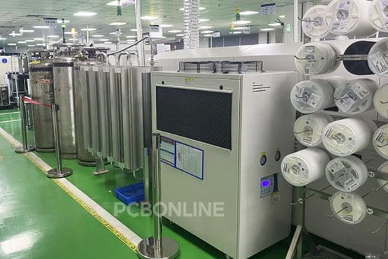
Solder paste management: Solder paste must be stored under refrigeration and allowed to warm up to ambient temperature before use. At PCBONLINE, we've upgraded to a smart solder paste management cabinet, which automatically stores, warms up, and records the solder paste for traceability. Failure to properly acclimate the paste can lead to moisture condensation, resulting in excessive solder balls and splattering during reflow.
Handling moisture-sensitive devices: We handle components designated as Moisture Sensitivity Level (MSL) 2 or higher according to J-STD-033. If they have exceeded their floor life, they must be baked before reflow to prevent internal moisture from expanding or even popcorning during the reflow process.
4. SMT stencil design
Precise solder paste printing heavily depends on the SMT stencil design. PCBONLINE has rich experience in SMT stencil design to ensure precise solder paste deposition onto the PCB copper pads. Most openings are designed 1:1 to the copper pads, but for ultra-small components, fine-pitch ICs, etc, we need to design their corresponding openings in the SMT stencil specially.
- For stencil openings corresponding to fine-pitch ICs and QFPs, we design the two ends of the aperture with rounded corners.
- For BGAs and ultra-small SMDs like 0402 and 0201, we design their stencil openings square-shaped.
- For stencil openings corresponding to QFN ground pads in a cross-shape ("+"), we ensure at least 0.5 mm clearance from the PCB pad edge.
- For USB, Mini USB, and CF/SD connectors, we extend the length in a 1:1.2 ratio to increase solder volume. To reduce stress and prevent solder beads, we use an inward concave opening method.
- We ensure enough stencil opening width to allow at least four solder balls to pass through.
![]()
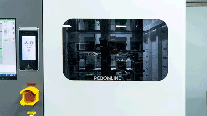
Dual-AOI to ensure reflow soldering success
At PCBONLINE, each of our SMT lines is equipped with two in-line AOI machines, before and after the reflow soldering process.
Both are three-dimensional optical inspections. The prior-reflow AOI checks the component placement and ensures no potential risks of tombstoning before reflow. The post-reflow AOI checks the PCBA surface to ensure no soldering defects after the reflow soldering process.
6. Nitrogen reflow soldering
Last but not least, if the PCBA is double-sided and easy to oxidize during reflow soldering, we can also provide nitrogen reflow to replace standard reflow soldering.
Partner with PCBONLINE for Full Turnkey PCB Assembly
PCBONLINE is a PCBA original equipment manufacturer providing full turnkey PCB assembly. We provide all the electronics manufacturing and materials used for our PCB box-build assembly services, including the PCB enclosures.
Our OEM PCBA manufacturing services offer:
- Complete procurement: We source and customize enclosures, cables, and accessories from reliable suppliers.
- Engineering support: We check enclosure and accessory designs for compatibility with your PCBA and can suggest design changes.
- Free DFM/DFT: We provide free Design for Manufacturability (DFM) and Design for Testability (DFT) checks to ensure that designs are optimized for a smooth production process.
- Special capabilities: IPX8 waterproof enclosures and encapsulation for rugged outdoor devices.
- Quality assurance: IPC-A-610 Class 3, automotive-grade or industrial-grade inspection standards.
- Turnkey delivery: From PCB fabrication to final product packaging and shipping.
- Testing and value-added services: Offering a range of quality assurance services, including X-ray inspection for hidden-joint PCBAs, first-article inspection, PCBA functional testing (FCT), IC programming, burn-in test, PCBA coating, enclosures, and box-build assembly.
Founded in 2005, our two advanced PCB manufacturing bases are in Jiangsu and Jiangxi Provinces, and our turnkey PCB assembly factory is in Shenzhen. Besides, we have an R&D team and a global supply network. We also maintain strategic cooperation with the top 3 fixture and enclosure factories in China to manufacture the custom PCBA fixtures and device enclosures.
PCBONLINE manufactures, assembles, and tests PCBs and PCBAs to box builds as a source factory manufacturer under one roof, from prototypes to bulky production, saving costs and time for you.
We keep strategic cooperation with the top 3 enclosure manufacturers in China to manufacture custom device enclosures.
We can design the PCB enclosure to match your PCB. Besides, we can help create user manuals, installation guides, and compliance labels.
Our high-quality PCBA contract manufacturing is certified with ISO 9001:2015, ISO 14001:2015, IATF 16949:2016, RoHS, REACH, UL, and IPC-A-610 Class 2/3.
Our one-on-one free and professional DFM helps you debug and improve design, to ensure the manufacturability, cost-effectiveness, and final device success.
Whether you need PCB box builds for consumer IoT devices, creative electronic products, automotive/medical-grade systems, etc, with 20 years of PCBA manufacturing and box build experience, we ensure that both electronics performance and final product presentation meet the highest standards. To get a quote for your full turnkey project, email us at info@pcbonline.com.
Conclusion
This article details the reflow soldering process and how to ensure the success of reflow soldering. From high-precision PCB fabrication to complete box-build production, PCBONLINE delivers high-quality PCBA manufacturing, including successful reflow soldering. Contact us to order full turnkey PCBA or box-builds for any mid to high-end applications.


