
A peelable solder mask, also known as a blue mask, is a positive plane (what you see is what you get in the design) used for the protection of the required pads in PCB assembly. A peelable solder mask layer is usually named GTPM and GBPM in design. Unlike the solder mask layer which is a negative plane in PCB design and covers the PCB permanently, the peelable solder mask is temporarily used in PCB manufacturing and assembly.
This post reveals details of peelable solder mask from the below content:
Part1: What is Peelable Solder Mask Used for
![]()
A peelable solder mask is a removable blue film that can withstand high temperaturesprinted on required PCB pads/holes at the end of PCB manufacturing. It serves to protect PCB pads/holes from oxidation and contamination. It is peeled off after SMT and THT assembly. The size of the peelable solder mask is the same as the pads or PTH holes it covers.
Some electronic components are thermally sensitive and can't withstand high temperatures of reflow soldering and wave soldering, so they need to be manually soldered after the SMT assembly and THT assembly. However, without a protection film, the bare copper of the pads and holes will be oxidized under high temperatures during reflow soldering and wave soldering. And we should keep in mind that pads and PTH holes can't be contaminated by solder paste or tin. So we need to print peelable solder masks to cover these pads and PTH holes.
After SMT assembly and THT assembly, the PCBA is assembled except for mounting the thermally sensitive components. Then these components will be manually assembled on the PCB boards.
Part 2: How does PCB Manufacturer Print Peelable Solder Mask
![]()
At PCBONLINE, we apply the peelable solder mask on the required PCB pads and PTH holes in the screen printing method. And the blue mask we use is Peters SD-2995.
When we confirm the PCB manufacturing requirements, if the boards require peelable solder masks, we manufacture custom stencils for printing blue masks on pads/holes according to the design.
If the NPTH or PTH holes need to be sealed by peelable solder masks, we also manufacture the custom tray that will plug in the holes at a depth of about 1/3 of the hole depth. The aim is to avoid the remains of the blue mask when peeling off.
The custom stencil and try are combined and placed in the screen printing machine, and then we print the blue mask on the PCBs panel by panel.
Then we bake the boards to let the blue mask dry and continue PCB manufacturing.
When we finish PCB manufacturing and testing, we place the circuit boards in the boxes. Between every two circuit boards, we put a piece of separator paper. This is because, without the separators, the peelable solder mask may stick to adjacent PCBs.
Part 3: Peelable Solder Mask VS High-Temperature Tape
![]()
Besides of peelable solder mask, the high-temperature tape is also used to protect the bare PCB pads, especially PCB gold fingers. Both peelable solder masks and high-temperature tapes can withstand high temperatures of reflow soldering and wave soldering. Then what are the differences between peelable solder masks and high-temperature taping?
Here are some differences between the two PCB pads coverage methods:
- Automation - The peelable solder mask is printed on PCBs automatically, while the high-temperature tape is applied manually.
- Efficiency - for batch production, a peelable solder mask is much more efficient than a high-temperature taping.
- Cost - for batch production, peelable solder masks cost less than high-temperature taping.
- Size - the maximum width of the peelable solder mask is 6mm. For coverage areas with a width of more than 6mm, it is better to use high-temperature tape.
For normal pads and PTH/NPTH holes that need coverage, the coverage size is usually small, and we print peelable solder masks; for PCB gold fingers, we usually use high-temperature tape to protect them from oxidation during reflow soldering and wave soldering.
Part 4: Peelable Mask PCB Capabilities
PCBONLINE is an advanced PCBA manufacturer that can meet your PCB manufacturing and assembly requirements, such as peelable solder masks, gold fingers, half holes, via-in-pads, etc. Founded in 1999, we have two large PCB manufacturing bases and one PCB assembly factory.
The capabilities of PCBs' peelable solder masks from the PCBA manufacturer PCBOINLINE are below.
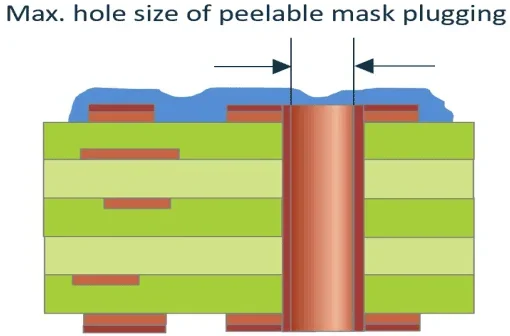
Maximum hole size of peelable mask plugging: 5mm
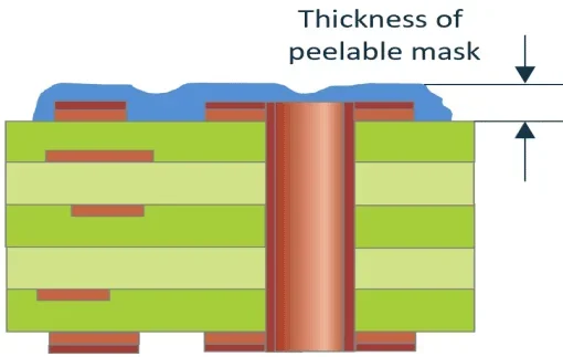
The thickness of peelable mask: 0.2mm-0.78mm
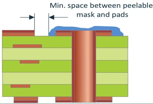
Min space between peelable soldermask and copper pads: 0.35mm
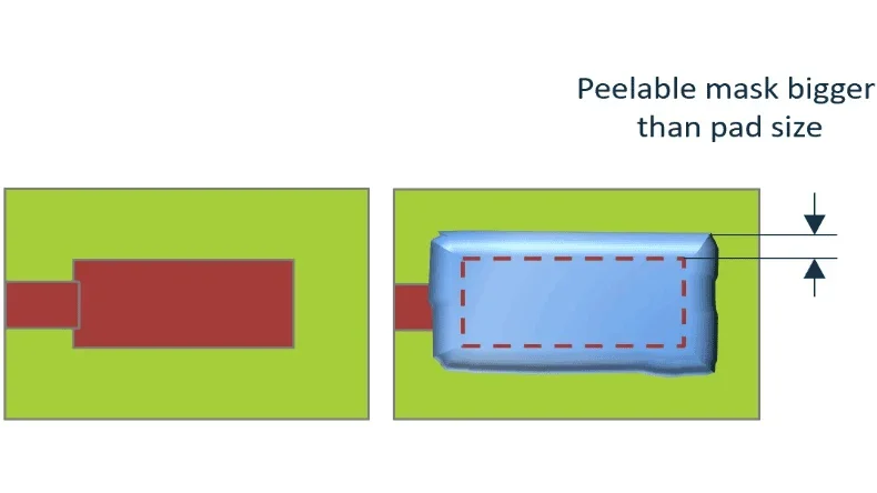
Peelable solder mask bigger than pad size (single side) 0.3mm
Both peelable solder masks and high-temperature tapes for PCB pad coverage are available at PCBONLINE.
PCBONLINE provides one-stop PCB manufacturing, including prototyping, batch PCB manufacturing and assembly, components sourcing, and testing.
You can order advanced PCBs from PCBONLINE, such as HDI PCBs, ceramic PCBs, high-frequency PCBs, clear flex PCBs, and aluminum PCBs.
We provide one-on-one engineering support throughout your PCB/PCBA project.
ISO 9001:2015, IATF 16949, UL, REACH, IPC, and RoHS-certified PCB/PCBA manufacturing quality management.
When the manufacturer PCBONLINE finishes PCB assembly, the peelable solder mask can be peeled off. Then we manually solder the rest components and conduct testing, or you can do it on your own. It depneds on you. If your PCB design has peelable solder mask requirements and you are looking for a one-stop PCB manufacturer, please feel free to contact us and send your Gerber/IPC-2581 by email at info@pcbonline.com.
Conclusion
A peelable solder mask is a removable film printed and baked on required PCB pads/holes, and it is used to cover the pads/holes to protect them from oxidation and contamination. PCBONLINE is a one-stop PCB manufacturer that can do peelable solder masks and high-temperature taping on PCBs. If you are looking for a cost-effective PCB/PCBA source factory that can satisfy PCB peelable solder mask needs, cooperate with the one-stop PCBA manufacturer PCBONLINE.


