
![]()
The surface mount is a technology called SMT - surface mount technology. This is a method of producing electronic circuits in which all the components are placed or "mounted" onto the surface of the printed circuit boards. The devices that are made using this method are called SMD - surface mount devices.
Over the years, this technology has replaced the method of using wires, to connect the different components. The wires are used to fit through holes into the circuit board. There are, however, some complex components that are not able to be handled by the surface mount technology and still use the old way. Good examples are the semiconductors and larger transformers.
The good thing here is that both types of technologies can fit on a single circuit board. The SMT technology has provided manufacturers with many ways to save space and for the final product, to be as compact as possible. On the other hand that is a big step for companies, which manufacture is related to any electronic devices.
The surface mount technology is a complex process and it depends on solder paste so the leads can connect to the right spots on the circuit boards. Over 50% of the failed board defects can be found in the improper use of solder paste printing .
In general, a stencil is printing the paste, then heats it, so it can fuse the connection. The amount of solder paste applied is critical. Over the years the components have become smaller and solder paste printing has become harder and harder. Little mistakes can cause malfunctioning, leading to a complete failure of the printed circuit boards.
Why is Solder Paste Printing so Important?
![]()
As you already know, the solder printing process is a major part of the SMT and it is responsible for most of the failures when it comes to PCBs. There is research that outlines that the solder paste volume is equally linked.
What I mean is:
Too much or too little paste is equal to an unreliable product.
The process aims to deposit the correct amount onto each of the pads that have to be soldered. As we already discussed this is of great importance. It is achieved by screen-printing the solder paste through a foil or stencil, but it can also be applied by jet printing.
Here are some of the key parameters that manufacturers have to follow very strictly to apply the paste effectively and accurately.
1. Squeegee Angle
2.
Squeegee Speed
3.
Squeegee Pressure
4.
Stencil Cleaning
5.
Stencil Speed
6.
PCB Support
7. Print Stroke and more…
Overall, the printing stage of the assembly process of PCB is essentially important. To achieve perfect quality and prevent any further issues, all of the above-presented aspects should be carefully considered. You can be sure that the manufacturers that are offering high-quality PCBs, follow all of these factors.
How to Select Solder Paste?
The key here is attention to detail. An assembly process is extremely complex and caprice. You have to make sure that you are using a suitable paste for your assembly process. There are many questions when it comes to picking the right soldering paste. Here is a simple and effective way to be sure that you are using the right paste for your needs.
1、 Make sure that your solder paste performs best with the materials you are working with. This way you will maximize performance, quality, and the heating processes during the manufacturing process.
2、 Be sure that the selected solder paste accommodates optimal heating methods and deposition.
3、 Do not save any money, especially when selecting a solder paste. Make sure that you purchase a high-quality paste because you can have serious issues if that process, in practice fails.
4、 Determine what properties and strengths are required to work best with the assembly.
5、 Get familiar with the different components and materials and determine which ones are most compatible.
6、 Last but not least, determine the preferred operating temperature and which soldering paste is optimal.
Knowing these key elements when choosing a solder paste will help you pick the right one. Do not forget to make the best decision when it comes to the solder paste alloy ratio: melting temperature, tensile strength, lead content, and allow powder particle size.
Solder Paste Inspection (SPI)
As per the research, 70% of the SMD soldering issues are coming from improper substandard solder pasting. Manufacturers can ensure their printing paste quality easily when they are producing small quantities. However, it becomes harder and harder by increasing the manufacturing amount of PCBs.
Here the SPI machines are coming to provide help. These machines utilize cameras that are capable of capturing 3D images and evaluating the quality of the solder paste factors such as height, alignment, volume, and more. This equipment can provide quick feedback regarding the quality of each board and provoke action from manufacturers for removal.
Overall, this process provides the manufacturers with a close and accurate observation of the solder printing process and also cuts down the cost of reworking bad units.
Find a Trusted Manufacturer
You probably already started to realize how important printing solder paste is, and that you need to make sure that you find a reliable manufacturer for it. Make sure that the manufacturer is familiar with the requirements of your electronic board or assembly.
PCBONLINE provides one-stop PCBs and their assembly. It is a reliable manufacturer.
Surface Mount Devices Components.
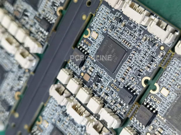
Surface mount technology and its devices (SMT/SMD) come in a variety of different sizes and packaging. These components are of great importance and most of them come in standard sizes so automated manufacturing can be easier.
Two of the most common components used are the surface mount capacitors and resistors. These SMD components come in small and compact packages ready for the manufacturing process.
Integrated Circuit Surface Mount Device Types and Spacing
In the PCB industry, there is a wide range of different mount devices and their spacing is suitable for particular uses. We will now review most of them:
-Quad Flat Pack (QFP) - It is a generic type for surface mount ICs. There are several different models.
- Low Profile Quad Flat Pack (LQFP) - The height is 1.4 mm and it has pins on all four sides.
- Plastic Quad Flat Pack (PQFP) It is mainly used for VLSI circuits and there is an equal number of gull-wing style pins on each side. There are 44 or more pins and narrow spacing.
There is also a Ceramic Quad Flat Pack and Thin Quad Flat Pack and they both are the same as PQFP , except for their base material and thickness.
-Ball Grid Array (BGA) - All of its contact pads are located beneath the device package. Their name comes from the fact that they appear as solder balls, before soldering.
-Thin Small Outline Package (TSOP) - It has a small pin spacing of 0.5 mm.
-Shrink Small Outline Package (SSOP) - This package has a pin spacing of 0.635 mm.
-Very Small Outline Package (VSOP) - One of the smallest packages with a spacing of 0.4, 0.5, or 0.65 mm.
These are just the most common packages, but it appears that there are many different types and sizes. However, the standard reduces that number to create the printed circuit board manufacturing easier with automation. Sometimes a custom design may require a specific method of manufacturing.
Component Placement
In the PCB assembly, for component placement, we will review the two major equipment machines required:
-
Pick & Place Machine
- Coming from its name, the machine's priority is to pick and place the components directly onto the bare board. Most probably this is the most fascinating machinery in the assembly industry. In general, this process is done by hand and this is where the standard sizing comes in handy. Whenever the components are of a standard size, a piece of equipment like this can be used, which will take less time and of course better quality. The pick-and-place machines are programmed to an enormous level of accuracy and it is impossible to make mistakes, unlike the human hand. They achieve amazing speeds and predetermined designs are the easiest to produce.
- Glue Machine - This is the hard part. The machines are accurate and place dots of glue on the board, where the components will sit. It is extremely hard to be done by hand and many issues were presented with this type of equipment. It is extremely helpful for double-sided PCBs!
- Soldering Machine - The PCBs have to pass through a wave of molten solder so the components get soldered. This is where the name of this machine comes from. At the beginning of the process, a layer of flux is applied to clean all the components so the solder can adhere. Then in the oven, a solder waveforms a connection between the component leads and contacts their respective holes.
Inspection
![]()
In-Circuit Testing - It is performed by a bed of nails fixture. This is the most common way to test if a PCB is fully functioning. The point of the “bed of nails” is for every of the PCB pins to create a contact and test its functionality. The PCBs have hundreds of test points and all of them can be tested at once with this equipment.
Automated Optical Inspection (AOI) - The human eye cannot catch defects as this machine can. The AOI machine uses high-definition cameras to capture the surface and build an analysis for its functionality. The analysis is extremely accurate and they follow exact guidelines. If the guideline is not met at any point the manufacturers have a detailed view of the issue and easily can identify how to resolve it.
Functional Validation Test (FVT) - This is the final test and it is deciding if the PCB is ready to go or not. This is the process where all PCBs are tested for hardware defects and now software is testing their performance. (Basically testing if they work). It is a simulation for the product in the environment in which it is going to be used.
PCB Manufacturing Environment
The PCB fabrication process is an extremely comprehensive and complex engineering technology that requires a clean and specific environment.
1.
The workshop has to be extremely clean and dust-free! Also, the air has to have a level of 100,000 cleanliness. PCBONLINE has 100,000 Levels of dust-free environment.
2. The temperature has to be (23-27) °C and the limit is 35 °C.
3. If the humidity in the air is too high, it can cause defects in the solder. On the other hand, if it is too low, the solvent in the flux will volatilize.
Conclusion
You now understand that the manufacturing process, including SMT, is an extremely caprice and complex procedure. PCBONLINE covers all of the requirements. It's not enough to have these hardware advantages. A strong technical team and after-sales customer service are the most important.
A team of experienced electronic engineers, an electronic engineer team with an average working experience of at least ten years, can communicate one-on-one online and assist customers from design to feasibility analysis to cost budget to solution implementation. The focus is to provide free technical consultation.
PCB usually has a few engineering problems, but the assembly of parts involves professional electrical engineering, IC selection, welding quality, and so on. After-sales is especially important, PCBONLINE has a professional after-sales team, and they are dedicated to success and quality.


