
Advantages of the PCB Layout Service Provider PCBONLINE
 MATERIALS
 Please provide PCBONLINE with schematics, sizes of enclosure/mechanical parts, BOM (bill of materials), and routing guidelines so that we can design the PCB for you. It's also okay for PCBONLINE to provide them.
 EQUIPMENT
 We use mainstream PCB design software including Allegro, Altium Designer, Protel, Autodesk Eagle, KiCAD, etc. PCBONLINE is equipped with complete production lines for PCB design and assembly.
 TEAM
TEAM PCBONLINE's R&D team can provide you with the best PCB layout service which will help design the most ingenious circuits for your products.
 QUALITY
 PCBONLINE has a standard mutual checking system and carries out sound DFM (Design for Manufacturing), DFA (Design for PCB Assembly), DFT (Design for Test), and DFX (Design for Excellence).
 CUSTOM
 Rich product development experiences in custom PCB layout for power supply, Arduino, Arduino Uno, audio effects, RFID, IoT, video monitoring, HD camera, video code, etc.
 EXPERTISE
 The R&D engineers at PCBONLINE have proficient theory and practical skills, EDA skills, and practical experience in signal integrity simulation and power source integrity analysis.
PCB Layout Process
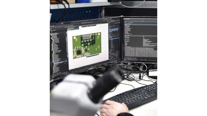
The steps of PCB design or PCB layout are similar whether you design on your own or from us. What makes the difference is experience. The general steps are:
Step 1. Draw the circuit board schematic.Step 2. Design PCB layout. At this step, you will determine the size of the circuit board, where to place the components, and how many layers of the board are.Step 3. The PCB layout software will automatically conduct wiring when you place the components.Step 4. Check your PCB layout and confirm.
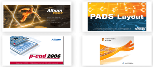
To draw the schematic and design a PCB layout, you also need PCB layout software. The commonly used software includes Altium Designer, Pads, OrCAD, Eagle, and P-CAD.
In Step 2, the PCB layout process can be more detailed:
Establish and confirm the design requirements, prepare the components information, and construct the databaseImport a netlistPerform functional simulation before synthesisDevelop a preliminary layout: conduct requirement analysis, evaluate the design, and make the design planOptimize the layout and confirmStart PCB wiringPerform post-synthesis functional simulationComplete all wiring manually and checkOptimize the wiringOutput the design.
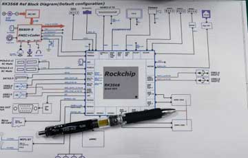
PCBONLINE has an R&D team including circuit designers, development engineers, MCU, and embedded system developers, and will help you design a complex circuit board perfectly. If you order from us you don't have to go through the above steps to get the final PCB layout, and you just need to provide us the circuit schematic, netlist, components information, and your design requirements.
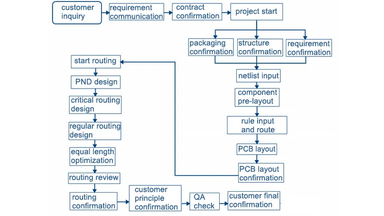
The workflow of PCB layout in PCBONLINE is: customer inquiries > submit data > quotation > payment > start to design > confirm > uploading > PCB layout download.
How to Generate Gerber Files
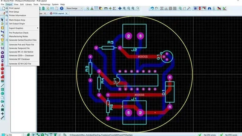
In PCB design, each layer of the PCB requires generating a Gerber file for the PCB manufacturer to understand. Gerber files in Altium Designer need to be generated through three outputs, the steps are as follows:
First output
Under the DXP menu bar, select "File" > "Fabrication Outputs" > 、“Gerber Files".Under the layer form, click "Plot Layers" and select "Used On".Click "OK" to complete the output.
Output again
In the layer form, select "Plot Layers"> "All off in Turn", and tick "Mechanical (x)" of the Layer name on the right.Set the following requirements under the Drill Drawing form: Under Drill Drawing Plots, select "Plot All Used Layer Pairs"; Under Drill Guide layer pairs, select "Plot All Used Layer Pairs".Click "OK" to complete the output.
The third output
Click "File" > "Fabrication Outputs" > "NC Drill Files", select "Leading/Trailing Zeroes" in the middle of the dialog box, and select "Suppress Leading Zeroes".Then click the "OK" button in the lower right corner. Complete the third output.
PCB Design Service Range and Process
PCBONLINE provides R&D and one-stop PCBA manufacturing. The PCB design services at PCBONLINE include:
Provide packaging dimensions of the PCB (you need to provide a datasheet of the components)Impedance calculation, stackup design, quality assurance check, technology check, and electromagnetic checkDesign PCBs to be FPC, HDI, rigid-flex, high-speed, high-frequency, high-power, analog, digital-analog, etc.Provide technical assistance, including schematic analysis, PCB design, electrical principle design error debugging, and DFA ensuring the quality and reliability of the design.
The materials provided to PCBONLINE for designing the PCB include:
Your schematic filePCB packing dimension file or component datasheetPCB structure file or structural restrictions, electrical design instructions, and precautions
Once the PCB design project starts, the PCB design service process of PCBONLINE goes on below.
The engineers from PCBONLINE have the schematic DRC check, structural verification, and other electrical design checks. We will report to you through the EQ (engineering question) record if any issues are found.During the project, PCBONLINE regularly sends the work progress documents to you for confirmation. You can have control of the PCB design status.After finishing the PCB layout, the engineers from PCBONLINE have mutual checks, including a PCB DFM check, QA check, and EMC check.After your confirmation of the PCB layout, we generate the Gerber and other production files.After your confirmation of the Gerber, the engineers at PCBONLINE output the assembly file, pick-and-place file, original PCB design file, Gerber, EQ records, etc.
PCB Design Service Capabilities
Applications of PCB design service:
Communication PCB design products: GSM/GPRS, switches, RF equipment, etc.Digital PCB design products: set-top boxes, HDTVs, digital cameras, camcorders, etc.Security PCB design products: Video surveillance, intercom, etc.Computer and related PCB design products: MB, NB, server, various industrial control boards, etc.
GET A FREE QUOTE
PCB and PCBA Certifications


Contact Our Expert Team Now

Learn about our products


Get customized services

 Phone
Phone WhatsApp
 Email
Email
Offer Electronics Manufacturing All-in-One
PCBONLINE® is a registered trademark or service mark of pcb online limited or its affiliates.
Copyright © 2005-2025 Pcb Online Limited. All rights reserved


