DFM, or Design for Manufacturing, is a set of design guidelines for developing PCBs (printed circuit boards) for production and assembly.
These PCB DFM guidelines aim to improve PCB manufacturing efficiency, and cost-effectiveness, and enhance product quality.
PCB DFM aims to improve product quality, simplify manufacturing, and reduce costs by considering production abilities and restrictions in the design stage.
It entails designing the PCB compatible with the procedures and producing tools to provide a continuing transition from design to manufacturing.
Crucial PCB DFM components include:
- Simplifying designs,
- choosing suitable materials,
- maximizing component location,
- assuring signal integrity,
- taking thermal considerations into account,
- and planning for simplicity of assembly and testing.
When to Implement the PCB DFM
The PCB layout process should begin with PCB DFM. You have the strength and latitude to make changes and improvements during the design process.
If you want to make design changes later on in the fabrication process, it is much more expensive and time-consuming to debug and repair production problems.
Why Does PCB DFM Matter
PCB DFM matters.
Implementing DFM successfully leads to increased reliability, decreased errors, and better manufacturability.
Cost reduction
PCB DFM can save production costs by addressing manufacturability issues at the PCB design stage. It aids in streamlining manufacturing, reducing fabric waste, and improving designs for cheaper manufacturing. Expensive rework can be avoided by identifying potential production issues by PCB DFM.
Efficient manufacturing
PCB DFM comprehensively considers component location, material choice, and adherence to the limitations and capabilities.
It makes the PCB manufacturing process methodical and more effective.
Decreased errors
DFM reduces the possibility of mistakes and production flaws.
A better product and less luxurious manufacturing errors result from the early identification and resolution of possible difficulties.
Improved product quality
PCB DFM improves the final product's quality and dependability.
DFM ensures that the PCB works as expected and has a longer lifespan by resolving layout faults that could result in flaws, errors, and overall performance issues.
Design for assembly and testing
PCB DFM strategies make sure the layout is simple to construct and check and streamline the assembly process and design for testability.
Signal integrity and thermal management
PCB DFM tackles critical issues relating to signal integrity and thermal management.
It guarantees that signals are transferred without degradation and that the PCB runs inside applicable temperature ranges.
Materials selection
DFM's main component is the selection of acceptable materials.
You can ensure that the PCB operates at its best by selecting materials that satisfy the electrical and thermal requirements of the application.
Advice For PCB DFM
Here is some advice for PCB DFM.
Cooperate often and early
Include the PCB fabrication and assembly teams right from the start of the design phase.
The ability to recognize and handle possible difficulties depends on regular communication between the design and manufacturing groups.
Follow design guidelines
Follow the design standards of the industry.
To guarantee a design that can be manufactured, these rules frequently include suggestions for trace widths, clearances, and other factors.
Make the design simpler
Maintain the PCB design's simplicity.
Try to reduce non-essential complexity because it can raise production costs and introduce problems. A simpler designs are more efficient and less expensive to build.
Select the right components
Try to select electronic components that can be produced in large quantities and are easily accessible for a lower production price.
Component price takes up most portion of the PCB assembly cost.
If you want to reduce the production cost, the best practice is to choose alternative components to replace the high-price components.
The one-stop PCB manufacturer PCBONLINE can help you choose alternative components that have the same functions and certificates to greatly reduce your costs in electronics manufacturing.
Consider materials carefully
Performance problems and shortened component life may result from overheating. You can address heat dissipation by:
- Ensuring correct airflow,
- employing heat sinks as necessary,
- and giving adequate thermal relief.
Design for test (DFT)
Create a PCB design that is simple to test and troubleshoot.
To simplify testing and cut expenses, include test points and access for probes.
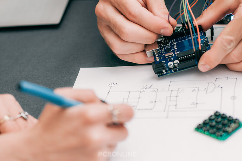
Iterate and prototype
Make PCB prototypes to test the concept before going into full production.
Make use of these prototypes to spot and resolve unanticipated production difficulties.
DFM software tools
Use DFM software tools to help early in the design process to detect potential production difficulties.
Training and expertise
Make sure your design and production teams have the DFM knowledge and experience they require.
Potential production problems are more likely to be identified by experienced engineers.
Common Issue of PCB DFM
Here are some common problems in PCB DFM.
Complex and overly dense designs
PCBs with excessive complexity, high component density, or restricted routing might be difficult to manufacture. They might make testing, soldering, and assembly more challenging.
You can use both sides of the HDI PCB to double the available space and increase the PCB size if it is okay.
Inadequate clearances and violations of design rules
If there are insufficient clearances between neighboring traces or between a trace and a close component, there is a chance of electrical interference or short circuits.
The use of too-narrow trace widths, too-small pads, or too-tight clearances are all examples of design violations. These infractions can affect the overall dependability and quality of the PCB.
The conductive components of the PCB, such as lines, pads, and PCB vias, need to have certain minimum clearances or spacings among those components to prevent accidental electrical connections.
Manufacturers, PCB design software, and industry standards all set the parameters for PCB design. These guidelines specify design factors, including trace widths, clearances, pad sizes, and other factors ensuring the PCB works properly.
Incorrect component and footprint selection
Electrical incompatibility might result when the chosen electronic components don't meet the circuit's electrical requirements or the planned functionality. The solution is us components with improper value or tolerance.
Improper component choice can cause mechanical incompatibilities. Check out to ensure the component's physical dimensions match the specified footprint to avoid problems with lead spacing.
Mismatched components can make positioning, soldering, and secure connection challenging. The physical dimensions and pin arrangement of the chosen component should match the footprint of the component on the PCB.
Placement of an unoptimized component
Improper component placement leads to too long trace lengths, a lot of bends, or ineffective routing pathways. They cause problems of electromagnetic interference (EMI) or signal distortion.
Besides, improperly positioned components can cause problems in signal, localized overheating, and assembly processes.
The solution is choosing components that fit the available area effectively and precisely positioning the heat-generating components.
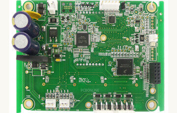
Inaccurate bill of materials (BOM)
In the context of PCB design, a Bill of Materials (BOM) is a document that lists the parts, materials, and quantities needed to manufacture the PCB assembly.
When the BOM identifies inaccurate components, leaves out crucial ones, or gives the wrong amounts, it may result in production delays, excessive ordering, or hurried component purchases, raising production costs.
To avoid these problems and guarantee a smooth PCB manufacturing process, efficient BOM management, thorough verification, and open communication between the design and procurement teams are crucial.
Lack of testability
The inability to be tested is a frequent problem in PCB DFM. Without specified test points and diagnostic tools, it is challenging to pinpoint certain problems.
Lack of testability arises when the practical features of testing and problem-solving are not sufficiently considered.
PCB designers must integrate testability elements into their designs, such as accessible test points and diagnostic interfaces.
Inadequate thermal management
The improper consideration of heat management is a typical problem in PCB DFM.
Misalignment of heat-generating parts, a lack of suitable heat sinks, and poor ventilation may cause localized overheating. This may shorten component life and cause reliability problems.
Besides, inadequate thermal management can render the PCB more vulnerable to heat stress, causing solder connection failures and PCB bending.
To solve these problems, precise component arrangement, the use of heat sinks and vias for heat dissipation, and appropriate ventilation designs are necessary.
Missing design for assembly (DFA) considerations
To make the PCB assembly process as effective and error-free as possible, DFA is a crucial component of PCB design.
It is crucial to apply DFA concepts to PCB design. This entails taking into account component positioning, clearances, and assembly-related access, as well as the design of features that make assembly easier.
Tight tolerances and non-standard parts
Very tight tolerances can make manufacturing complex and expensive. If the application's requirements don't support strict tolerances, it might cause problems with component alignment and soldering.
Additionally, using bespoke or non-standard parts might lengthen lead times and raise production costs.
To solve this problem, PCB designers should consider the standards and tolerances required for their particular application and refrain from requiring excessive accuracy.
Designers should make sure that non-standard parts are accessible.
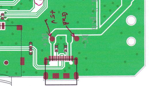
No solder mask between pads

Solder mask avoids contact between copper and other metals. Without a solder mask in between the pads, contact between negatively charged metals might emerge, leading to unforeseen short circuits.
Include this in the design guidelines for all of your PCB manufacturers to guarantee that each circuit board has enough solder masks.
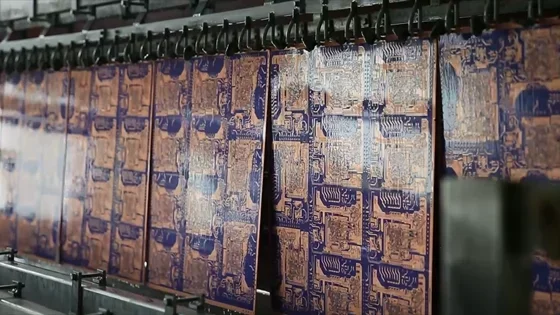
Insufficient accounting for manufacturing processes
Production issues might come from the PCB design's failure to take into account the limitations and capabilities of the manufacturing equipment.
Designers and manufacturing teams should work closely together, including their knowledge early in the design phase, to solve this problem. A smoother PCB manufacturing process may be achieved by designers by anticipating manufacturing processes and mitigating possible problems.
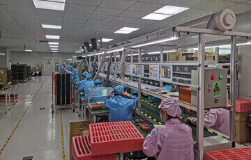
One-Stop PCB Manufacturer Providing PCB DFM
If you want to ensure PCB DFM and electronics manufacturing success, you can work with a one-stop PCB manufacturer PCBONLINE.

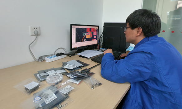
PCBONLINE has its R&D team to provide one-stop solutions for your product concept, offer free PCB DFM, Gerber/BOM check, or take part in the R&D of your project's early design stage.
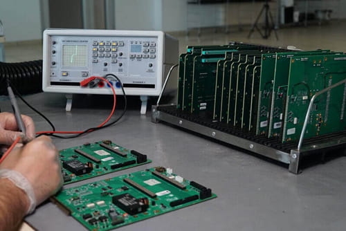
Founded in 1999, PCBONLINE is an electronic manufacturing services (EMS) PCB manufacturer with two large advanced PCB manufacturing bases and one PCB assembly factory.
The professionals at PCBONLINE provide free and comprehensive checks to ensure your project's manufacturability even though you don't have PCB DFM.
PCBONLINE has strong R&D capabilities. Whether you have PCB design or not, PCBONLINE can provide electronics manufacturing for you.
PCBONLINE provides one-on-one engineering support and can reduce your electronic costs with an optimal PCB design.
PCBONLINE has rich experiences in choosing alternative components with the same functions and certification to reduce your spending on electronic components.
PCBONLINE focuses on details and quality. Its PCB fabrication and assembly can be military and medical electronics grade.
Are you ready for PCB DFM and going forward further like PCB fabrication, PCB assembly, or finished product assembly? Contact PCBONLINE by email at info@pcbonline.com.
Conclusion
PCB DFM is a collection of design guidelines for printed circuit boards and is intended to optimize PCB manufacturing efficiency and cost-effectiveness. This blog advises on PCB DFM ensuring manufacturing success and lists common issues and suggestions. If you want to ensure the correctness of your PCB design, you can chat with the professionals at PCBONILNE from the window on the right.
PCB fabrication process.pdf