Round PCBs are printed circuit boards designed in a circular shape, deviating from the traditional square or rectangular designs. Round PCBs offer several advantages in specific applications. This blog reveals everything about round PCBs, including how to design and profile round PCBs of diverse types.
Advantages of Round PCB
One notable advantage of round PCBs is their efficient use of space. In devices or systems where space optimization is critical, such as in small electronics like smartwatches, sensors, or compact gadgets, round PCBs allow for a more streamlined and compact arrangement of components. This unique shape minimizes unused space and can lead to more efficient and aesthetically pleasing designs.
Another advantage is their improved signal integrity. The absence of sharp corners reduces the risk of signal distortion and electromagnetic interference (EMI), especially at higher frequencies. This makes round PCBs ideal for applications requiring stable and clear signal transmission, such as IC substrate and test boards, radio frequency (RF) devices, antennas, and communication systems. The circular layout allows for more direct and efficient signal paths, enhancing performance and reliability.
Additionally, round PCBs are often used in applications involving rotational movement. Devices like motor controllers, drones, and robotic systems frequently utilize round PCBs because the circular shape accommodates rotational movement more naturally. By aligning components along the circular perimeter, these PCBs facilitate smoother rotation without the risk of damaging or entangling wires and components.
Overall, the round PCB design offers a practical solution for specific applications where space efficiency, signal integrity, and rotational movement compatibility are essential design considerations.
Types of Round PCB
Printed circuit boards of all materials can be made round PCBs, including aluminum LED PCBs, FR4 PCBs, ceramic PCBs, and many more.
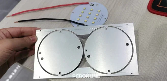
An aluminum round PCB is typically designed for LED applications. These PCBs are excellent for dissipating heat generated by high-power LEDs, ensuring optimal thermal management.
An FR4 round PCB is a circular printed circuit board made from FR4, a flame-retardant material widely used in electronics manufacturing. FR4 PCBs offer excellent electrical isolation properties and durability and are suitable for many applications.
A ceramic round PCB is a circular printed circuit board made from ceramic materials like aluminum oxide (Al2O3) or aluminum nitride (AlN). Ceramic PCBs have exceptional thermal conductivity, excellent electrical insulation, and high mechanical strength.
Ceramic PCBs are ideal for applications requiring high-temperature resistance and reliability, such as high-power electronic devices, aerospace systems, and medical equipment.
Besides, there are copper-based round PCB, flexible round PCB, high-frequency round PCB, etc.
How to Design a PCB to be Round in Proteus
Although designing a round PCB in Proteus can be a complex task, with the right guidance, it becomes much more manageable.
In this tutorial, we are going to see the step-by-step guide to designing a round PCB in Proteus.
Step 1: Create your schematic
1. Launch Proteus
Run the Proteus program and create a new project by clicking on "File", then click on "New Project" from the sub-menu.
2. Design Your Circuit
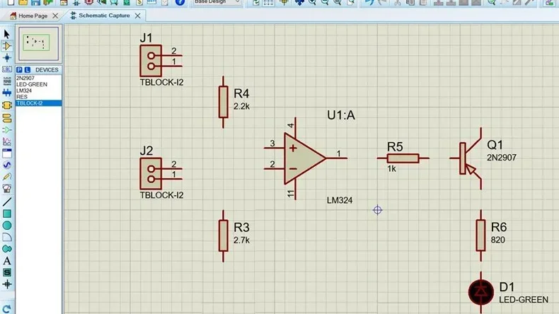
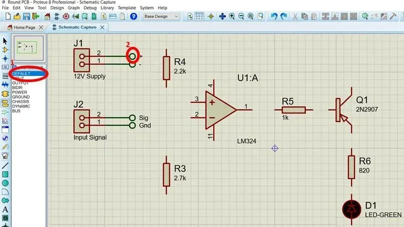
The next step is constructing a schematic diagram of the circuit. For this tutorial, an op-amp-based comparator.
Design your circuit schematic by dragging and dropping electronic components from the component library.
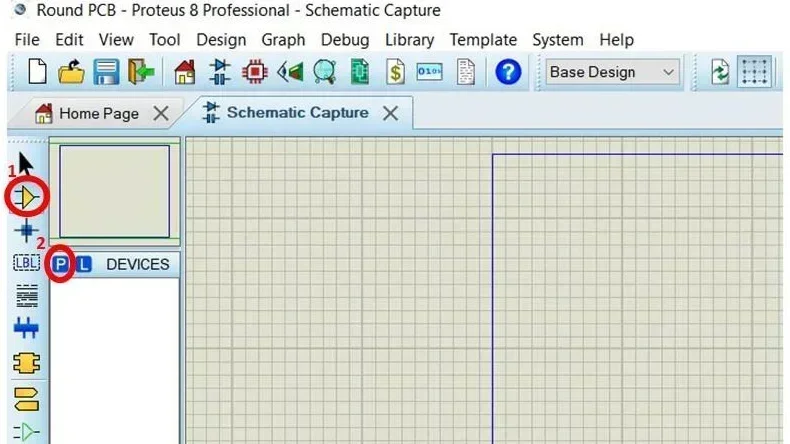
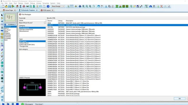
The component library can be accessed by pressing "Component mode" and pressing "P" on the left menu bar as demonstrated in the next figure.
The component library looks like the image below.
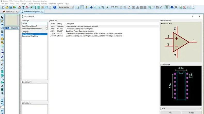
Now, find all the required components and add them one by one. We will need op-amp, resistor, transistor, LED, and connectors. You can change them according to your requirements.
The figure below represents the placement of different components.
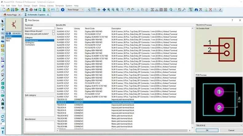
The terminal blocks are connected with default terminals. You can find them in "Terminal" mode and place them as shown above. Then change the names of each terminal as represented in the above circuit.
The next step is to connect these components using wires. Ensure that your schematic is error-free before proceeding to the PCB design. Your circuit should look like the following figure.
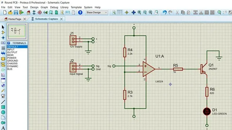
Step 2: Verify and simulate your circuit
This step is optional. You can simulate the circuit in Proteus by connecting batteries and input sinusoidal waves. The two terminal blocks are for the AC and DC powers.
As this is a comparator circuit, it will turn the LED On when the input voltage exceeds a certain limit. This limit is determined by R3 and R4 using the voltage divider formula.
Step 3: Switch to PCB layout mode
Once your schematic is error-free, switch to PCB layout mode by clicking on the "Ares" button shown in the next image.
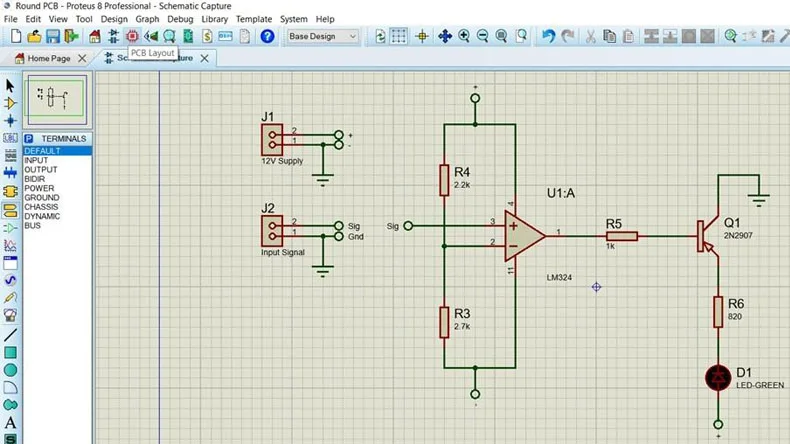
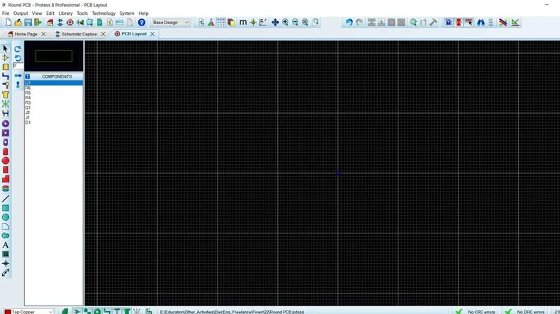
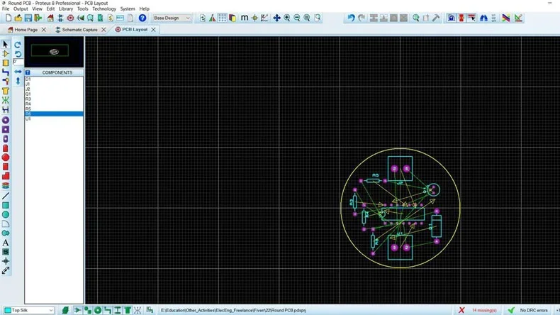
A new window will open for the PCB layout and will look like the following one.
Step 4: Design your PCB layout
1. Import Components
Proteus will automatically import components from your schematic. You'll see them listed on the left side of the Ares window.
2. Draw the boundary
Now, draw the round boundary of the PCB. The right layer should be selected from the layer menu given in the options at the bottom. The "Board edge" layer should be selected as shown in the next figure.

Then, select the circle shape from the "2D Graphics Circle Mode" as shown below.
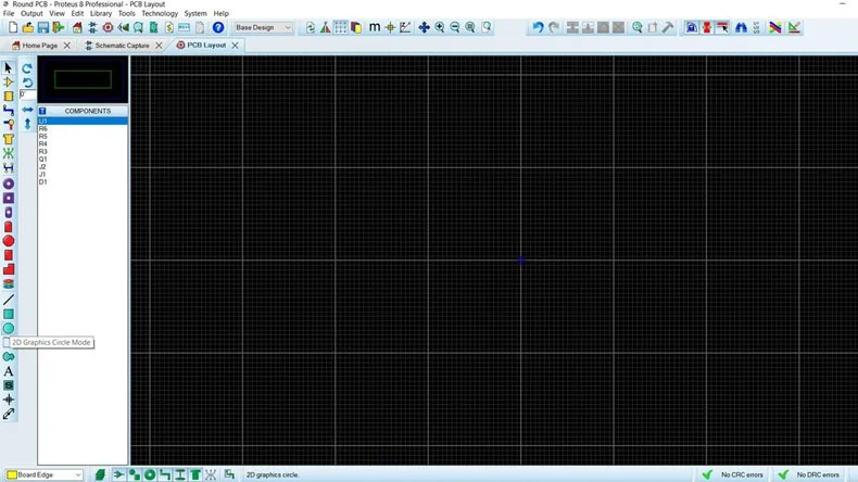
Draw a circle of any size and then edit the properties to set the right dimensions of the circle.
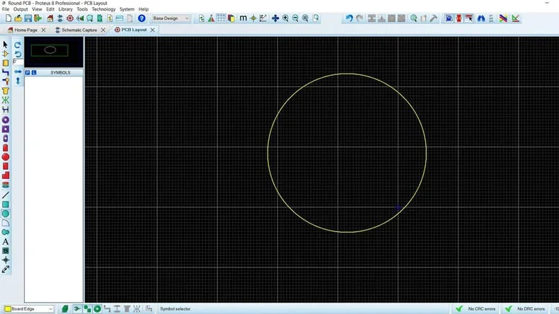
For this tutorial, we select a radius of 25mm with X and Y coordinates to be 0, for the circle as it is feasible for the given components and their size.
3. Place Components
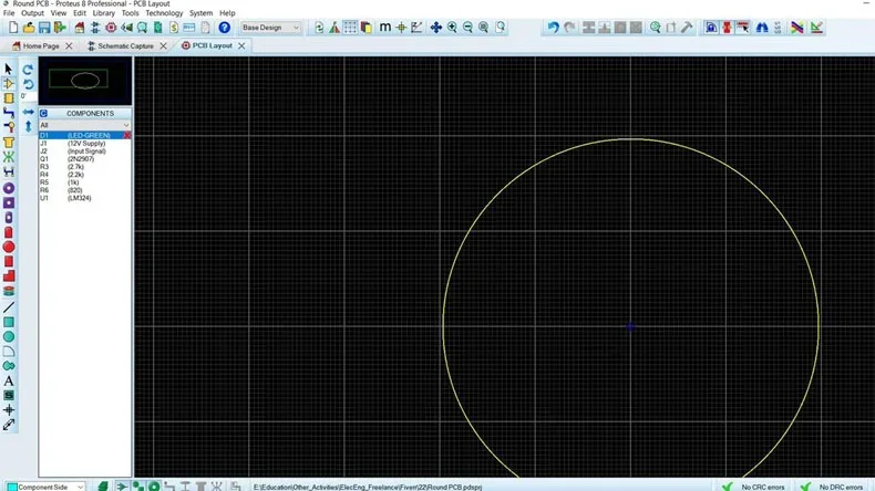
Now when we have the board edge boundary, we will drag and drop components onto the PCB layout grid.
The components should be placed logically, considering the connections and spacing. The component will be selected from the "Component mode" and you will see a small red cross in front of the LED.
This cross indicates that this component does not have a PCB model attached to it. As the LED we are using has the same footprint as a diode, we will add the diode footprint. You can use any footprint that has the same dimensions as your physical component.
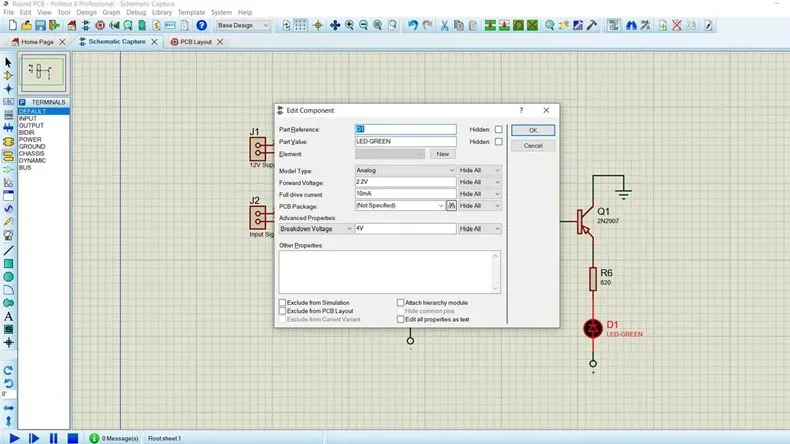
The following image shows the process of adding a footprint after getting into the Ares for PCB designing. For this, we will need to go back to the schematic portion. Then double-click the LED. Then look for the viable footprint and add it.
Now get back into PCB mode. Add all the components one by one.
4. Route Connections
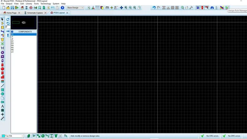
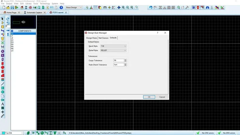
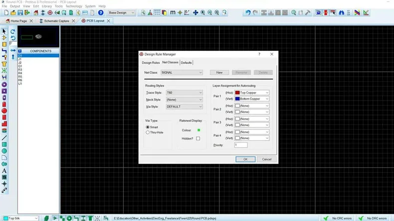
Now it’s time for routing. Click the "Design Rule Manager" to set the properties of the track.
Set the properties as below.
After setting the properties of the tracks, you can place each track and do the manual routing. But before that, it is important to check the design rule.
Step 5: Design Rule Check (DRC)
Before finalizing your design, run the Design Rule Check (DRC) to ensure your PCB layout adheres to standard design rules. Click on "Check" -> "Design Rule Check" and fix any errors or warnings reported by the DRC.
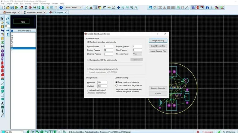
Step 6: Routing
For a quick outcome, we will use the auto-routing tool of Proteus. The Auto-routing option is present near the Design Rule Manager. Click the "Begin Routing" option and see the magic happen!
Step 7: Finalize your design
Save your Proteus project to ensure you can come back and make changes if necessary.
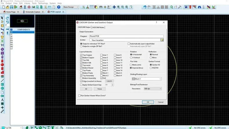
Step 8: Generate Gerber files
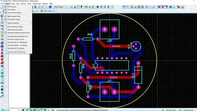
Gerber files are industry-standard files used by PCB manufacturers. Go to "File" -> "Export" -> "Gerber" to generate Gerber files for your PCB design. Follow the prompts and select the appropriate options.
You've successfully designed a round PCB in Proteus. Remember that PCB design can be complex, and attention to detail is crucial. Always double-check your connections, follow design rules, and simulate your circuit before proceeding with the PCB layout.
One-Stop Round PCB Manufacturing at PCBONLINE
Once you have the Gerber files, you can send them to a PCB manufacturer to produce your custom round PCB. PCBONLINE, a one-stop PCB manufacturer, provides high-quality and affordable PCB fabrication, PCB assembly, and value-added services on your demand.
PCBONLINE, founded in 1999, has two large advanced PCB manufacturing bases, one PCB assembly factory, and an R&D team that provides design solutions. If you have any doubts in round PCB design, electronics manufacturing, and end product issues, PCBONLINE can offer help.
PCBONLINE is an electronic manufacturing service (EMS) supplier offering round PCB and finished products under your brand.
At PCBONLINE, you can have your round PCBs manufactured to be FR4, aluminum, copper-based, ceramic, high-frequency, HDI, flexible, rigid-flex, hybrid-substrate, or transparent.
Cost-effective round PCB fabrication and assembly from prototypes to bulk production at one stop.
The professionals at PCBONLINE provide one-on-one engineering support and customer service throughout the project.
The round PCB and PCBA at PCBONLINE are certified with ISO 9001: 2015, IATF 16949, RoHS, REACH, UL, and IPC.
Over the many years, PCBONLINE has fabricated and assembled all types of rounded PCBs for many applications in the industrial, automotive, communication, computer, consumer, defense, medical, and aerospace industries.
Are you ready for round PCB and PCBA manufacturing? You can contact PCBONLINE at info@pcbonline.com.
How does PCB Manufacturer Profile Round PCB
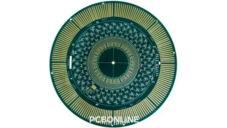
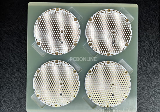
Typically, round PCBs are panelized on a panel for PCB fabrication and assembly. After the PCB assembly, the PCB manufacturer de-panels them to be single ones.
How does a PCB manufacturer profile the circular PCBs and de-panel them?
The PCB manufacturer PCBONLINE profiles and de-panels round PCBs by V-cuts, mechanical routing/CNC (computer numerical control), and laser-cuts.
Round FR4 and aluminum PCBs
For round FR4 PCBs and aluminum PCBs, the manufacturer typically uses a method called V-cut machining to profile them. In this process, a V-shaped groove is created along the desired separation line on the PCB panel. The V-cut penetrates partially through the PCB material, allowing for easy separation of the individual round PCBs after the cutting process. Careful control of the cutting depth and precision of the V-cut ensures clean and accurate separation, resulting in round PCBs ready for further assembly and use.
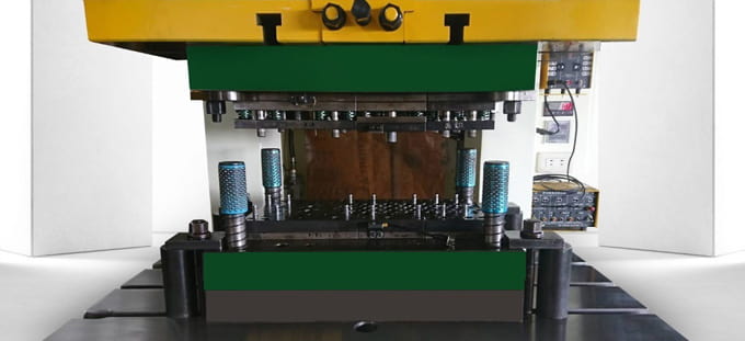
After the PCB assembly, round FR4 PCBs and aluminum PCBs are de-paneled by mechanical routing or CNC equipped with rotary cutting tools. Aluminum PCBs do not allow burrs, and the manufacturer PCBONLINE attaches protective films on the PCB before routing. The cutting tool, guided by computer-controlled programming, precisely follows the outline of the circular PCBs, effectively separating them from the panel without causing any damage to the boards.
During the profile and de-paneling of the round PCBs, the hardness of the milling cutter required for aluminum PCBs is larger than that for FR4 PCBs.
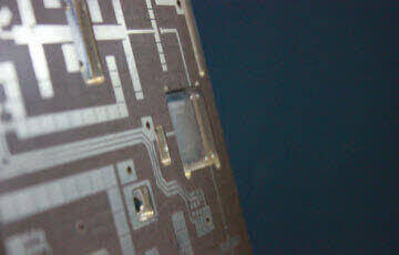
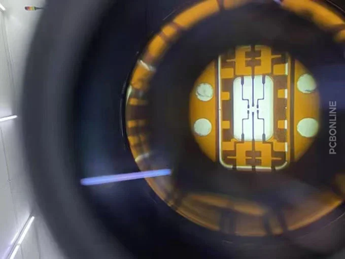
Round ceramic PCBs
The PCB manufacturer uses the laser cutting method to profile and de-panelize round ceramic PCBs.
In this process, the circular PCBs are placed on a stable platform, and a high-powered laser beam is directed onto the material. The laser energy is precisely controlled to cut through the ceramic substrate along the predefined circular outline. At the laser head, the PCB manufacturer installs a nitrogen spout to protect the nearby ceramic materials and circuit traces.
The focused laser beam vaporizes the ceramic material, creating a clean and precise cut without causing damage to the delicate components or circuits on the board. This method ensures accuracy and minimizes stress on the PCB, making it a preferred choice for de-paneling round ceramic PCBs in manufacturing processes.
Post-de-paneling, the individual round PCBs undergo thorough quality checks to guarantee they meet the required specifications before being used in electronic devices.
Conclusion
This blog comprehensively introduced round PCBs, from design to the diverse types and the de-paneling processes. Round PCBs demand careful layout, component placement, and routing within the given circular form. The PCB types, ceramic, FR4, aluminum LED PCBs, and many more, cater to different application needs, offering versatility in electronic device design. Besides, this blog presented a one-stop PCB manufacturer that provides high-quality and affordable round PCBs and their assembly. If you want on-the-demand round PCBs, you can talk to PCBONLINE directly from the chat window on the right.
PCB fabrication at PCBONLINE.pdf